Transcription of Parallel Control - psemi.com
1 2012-2016, 2018 pSemi Corp. All rights reserved. Page 1 of 21 Document No. DOC-16514-8 | Product Description The PE43704 is a HaRP technology-enhanced, high linearity, 7-bit 50 RF Digital Step Attenuator (DSA). It offers maximum power handling of 28 dBm up to 8 GHz and covers a dB attenuation range in dB, dB, or dB steps. The PE43704 is a pin-compatible version of PE43703. It provides multiple CMOS Control interfaces and an optional VssEXT bypass mode to improve spurious performance. It maintains high attenuation accuracy over frequency and temperature and exhibits very low insertion loss and low power consumption. No blocking capacitors are required if DC voltage is not present on the RF ports. The PE43704 is manufactured on Peregrine s UltraCMOS process, a patented variation of silicon-on-insulator (SOI) technology on a sapphire substrate, offering the performance of GaAs with the economy and integration of conventional CMOS.
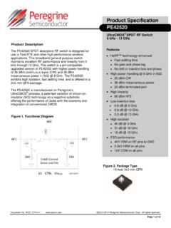
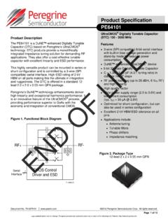
2 PE43704 Figure 2. Functional Diagram Features HaRP technology enhanced Safe attenuation state transitions Attenuation options: covers a dB range in dB, dB, or dB steps dB monotonicity for 6 GHz dB monotonicity for 7 GHz dB monotonicity for 8 GHz High power handling @ 8 GHz in 50 28 dBm CW 31 dBm instantaneous power High linearity IIP3 of 61 dBm Control logic Programming modes Direct Parallel Latched Parallel Serial Serial Addressable High-attenuation state @ power-up (PUP) ESD performance HBM on all pins Product Specification UltraCMOS RF Digital Step Attenuator, 7-bit, dB with Optional VssEXT Bypass Mode 9 kHz - 8 GHz Figure 1. Package Type 32-lead 5x5 QFN Control Logic InterfaceRF InputRF OutputSwitched Attenuator ArraySerial InLECLKA0A1A2 Parallel Control7P/SVssEXT (optional)DOC-02161 Document No.
3 DOC-16514-8 | UltraCMOS RFIC Solutions Page 2 of 21 2012-2016, 2018 pSemi Corp. All rights reserved. PE43704 Product Specification Table 1. Electrical Specifications: dB steps @ +25 C, VDD = to , VssEXT = 0V or VDD = to , VssEXT = (ZS = ZL = 50 ) unless otherwise noted Notes: 1. The input 1dB compression point is a linearity figure of merit. Refer to Table 5 for the RF input power PIN (50 ) 2. To prevent negative voltage generator spurs, supply volts to VssEXT Parameter Condition Frequency Min Typ Max Unit Operating frequency 9 kHz 6000 MHz As shown Attenuation range dB Step 0 dB Insertion loss 9 kHz 2 GHz 2 GHz 4 GHz 4 GHz 6 GHz dB dB dB Attenuation error 9 KHz 4 GHz + ( + of Attenuation Setting) - ( + 2% of Attenuation Setting) dB dB 0 dB dB Attenuation settings 4 GHz 6 GHz + ( + 6% of Attenuation Setting) - ( +1% of Attenuation Setting) dB dB 16 dB dB Attenuation settings 9 KHz 4 GHz + ( + of Attenuation Setting) - ( + of Attenuation Setting) dB dB 4 GHz 6 GHz + ( + of Attenuation Setting)
4 - ( +1% of Attenuation Setting) dB dB Return loss Input port 9 kHz 4 GHz 4 GHz 6 GHz 20 15 dB dB Return loss Output port 9 kHz 4 GHz 4 GHz 6 GHz 17 13 dB dB Relative phase 0 dB dB Attenuation settings 9 kHz 6 GHz 58 deg Input 1dB compression point1 50 MHz 6 GHz 32 34 dBm IIP3 Two tones at +18 dBm, 20 MHz spacing 50 MHz 6 GHz 61 dBm Typical spurious value2 VssEXT = 0V 140 dBm RF Trise/Tfall 10% / 90% RF 600 ns Settling time RF settled to within dB of final value 2 s Switching time 50% CTRL to 90% or 10% RF s PE43704 Product Specification 2012-2016, 2018 pSemi Corp. All rights reserved. Document No. DOC-16514-8 | Page 3 of 21 Table 2. Electrical Specifications.
5 DB steps @ +25 C, VDD = to , VssEXT = 0V or VDD = to , VssEXT = (ZS = ZL = 50 ) unless otherwise noted Parameter Condition Frequency Min Typ Max Unit Operating frequency 9 kHz 7000 MHz As shown Attenuation range dB Step 0 dB Insertion loss 9 kHz 2 GHz 2 GHz 4 GHz 4 GHz 6 GHz 6 GHz 7 GHz dB dB dB dB Attenuation error 0 dB dB Attenuation settings 9 KHz 4 GHz + ( + of Attenuation Setting) - ( + 2% of Attenuation Setting) dB dB 4 GHz 7 GHz + ( + of Attenuation Setting) - ( +1% of Attenuation Setting) dB dB 9 KHz 4 GHz + ( + of Attenuation Setting) - ( + of Attenuation Setting) dB dB 16 dB dB Attenuation settings 4 GHz 7 GHz + ( + of Attenuation Setting) - ( + of Attenuation Setting) dB dB Return loss Input port 9 kHz 4 GHz 4 GHz 7 GHz 20 16 dB dB Return loss Output port 9 kHz 4 GHz 4 GHz 7 GHz 17 14 dB dB Relative phase 0 dB dB Attenuation settings 9 kHz 7 GHz 65 deg Input 1dB compression point1 50 MHz 7 GHz 32 34 dBm IIP3 Two tones at +18 dBm, 20 MHz spacing 50 MHz 7 GHz 61 dBm Typical spurious value2 VssEXT = 0V 140 dBm RF Trise/Tfall 10% / 90% RF 600 ns Settling time RF settled to within dB of final value 2 s Switching time 50% CTRL to 90% or 10% RF s Notes: 1.
6 The input 1dB compression point is a linearity figure of merit. Refer to Table 5 for the RF input power PIN (50 ) 2. To prevent negative voltage generator spurs, supply volts to VssEXT Document No. DOC-16514-8 | UltraCMOS RFIC Solutions Page 4 of 21 2012-2016, 2018 pSemi Corp. All rights reserved. PE43704 Product Specification Table 3. Electrical Specifications: 1 dB steps @ +25 C, VDD = to , VssEXT = 0V or VDD = to , VssEXT = (ZS = ZL = 50 ) unless otherwise noted Parameter Condition Frequency Min Typ Max Unit Operating frequency 9 kHz 8000 MHz As shown Attenuation range 1 dB Step 0 - 31 dB Insertion loss 9 kHz 2 GHz 2 GHz 4 GHz 4 GHz 6 GHz 6 GHz 8 GHz dB dB dB dB Attenuation error 0 dB 15 dB Attenuation settings 9 kHz 4 GHz + ( + of Attenuation Setting) - ( + 2% of Attenuation Setting) dB dB 4 GHz 7 GHz + ( + 6% of Attenuation Setting) - ( + 2% of Attenuation Setting) dB dB 7 GHz 8 GHz + ( + 7% of Attenuation Setting) - ( + 2% of Attenuation Setting)
7 DB dB 9 kHz 4 GHz + ( + of Attenuation Setting) - ( + of Attenuation Setting) dB dB 16dB 31 dB Attenuation settings 4 GHz 7 GHz + ( + of Attenuation Setting) - ( + 3% of Attenuation Setting) dB dB 7 GHz 8 GHz + ( + 7% of Attenuation Setting) - ( + 4% of Attenuation Setting) dB dB Return loss Input port 9 kHz 4 GHz 4 GHz 8 GHz 20 dB dB Return loss Output port 9 kHz 4 GHz 4 GHz 8 GHz 17 dB dB Relative phase 0 dB 31 dB Attenuation settings 9 kHz 8 GHz 80 deg Input 1dB compression point1 50 MHz 8 GHz 32 34 dBm IIP3 Two tones at +18 dBm, 20 MHz spacing 50 MHz 8 GHz 61 dBm Typical spurious value2 VssEXT = 0V 140 dBm RF Trise/Tfall 10% / 90% RF 600 ns Settling time RF settled to within dB of final value 2 s Switching time 50% CTRL to 90% or 10% RF s Notes: 1.
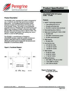
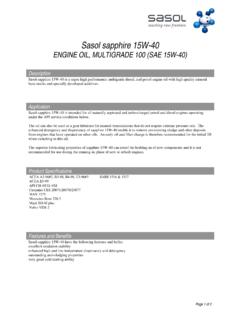
8 The input 1dB compression point is a linearity figure of merit. Refer to Table 5 for the RF input power PIN (50 ) 2. To prevent negative voltage generator spurs, supply volts to VssEXT PE43704 Product Specification 2012-2016, 2018 pSemi Corp. All rights reserved. Document No. DOC-16514-8 | Page 5 of 21 Figure 3. Pin Configuration (Top View) Pin # Pin Name Description 1 N/C No connect 2 VDD Supply voltage 3 P/S Serial/ Parallel mode select 4 A0 Address bit A0 connection 5, 6, 8-17, 19 GND Ground 7 RF11 RF1 port (RF input) 18 RF21 RF2 port (RF output) 20 VssEXT2 External Vss negative voltage Control 21 A2 Address bit A2 connection 22 A1 Address bit A1 connection 23 LE Serial interface latch enable input 24 CLK Serial interface clock input 25 SI Serial interface data input 26 C16 (D6)3 Parallel Control bit, 16 dB 27 C8 (D5)3 Parallel Control bit, 8 dB 28 C4 (D4)3 Parallel Control bit, 4 dB 29 C2 (D3)3 Parallel Control bit, 2 dB 30 C1 (D2)3 Parallel Control bit, 1 dB 31 (D1)3 Parallel Control bit, dB 32 (D0)
9 3 Parallel Control bit, dB Pad GND Exposed pad: ground for proper operation Table 4. Pin Descriptions Notes: 1. RF pins 7 and 18 must be at 0V DC. The RF pins do not require DC blocking capacitors for proper operation if the 0V DC requirement is met 2. Use VssEXT (pin 20) to bypass and disable internal negative voltage generator. Connect VssEXT (pin 20) to GND (VssEXT = 0V) to enable internal negative voltage generator 3. Ground , , C1 C2, C4, C8, C16 if not in use Notes: 1. Normal mode: connect VssEXT (pin 20) to GND (VssEXT = 0V) to enable internal negative voltage generator 2. Bypass mode: use VssEXT (pin 20) to bypass and disable internal negative voltage generator 3. 100% duty cycle, all bands, 50 4. Pulsed, 5% duty cycle of 4620 s period, 50 Table 5.
10 Operating Ranges Parameter Symbol Min Typ Max Unit Supply voltage (normal mode, VssEXT = 0V)1 VDD V Supply voltage (bypass mode, VssEXT = , VDD for full spec. compliance)2 VDD V Negative supply voltage (bypass mode)2 VssEXT V Supply current (normal mode, VssEXT = 0V)1 IDD 130 200 A Supply current (bypass mode, VssEXT = )2 IDD 50 80 A Negative supply current (bypass mode, VssEXT = )2 ISS -40 -16 A Digital input high VIH V Digital input low VIL V Digital input current ICTRL 15 A RF input power, CW3 9 kHz < 50 MHz 50 MHz 8 GHz PMAX,CW see Fig. 4 +28 dBm dBm RF input power, pulsed4 9 kHz < 50 MHz 50 MHz 8 GHz PMAX,PULSED see Fig. 4 +31 dBm dBm Operating temperature range TOP -40 25 +85 C 8765432124232221201918173231302928272625 161514131211109 Exposed Ground PadN/C VDD P/S A0 GND GND RF1 GND GND GND GND GND GND GND GND CLK LE A1 A2 VssEXT GND RF2 GND C1 C2 C4 C8 C16 SI Pin 1 dot marking GNDD ocument No.


![-'3BPU#DPBO ]HXBIZJ) F JYJ%/PSUI](/cache/preview/6/7/6/f/b/9/2/b/thumb-676fb92b022decbfab7d387be6a97bb5.jpg)