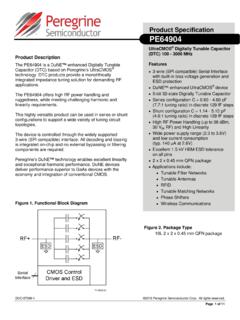
Transcription of Product Specification PE42540 - pSemi
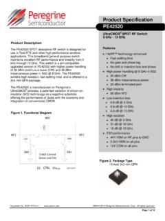
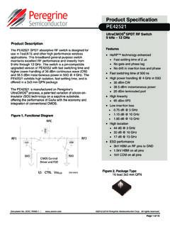
1 2010-2022 pSemi Corporation All rights reserved. Page 1 of 12 Document No. DOC-77985-6 | Features HaRP technology enhanced Fast settling time Eliminates gate and phase lag No drift in insertion loss and phase High linearity: 58 dBm IIP3 Low insertion loss: dB @ 3 GHz, dB @ 6 GHz and dB @ 8 GHz High isolation: 45 dB @ 3 GHz, 39 dB @ 6 GHz and 31 dB @ 8 GHz Maximum power handling: 30 dBm @ 8 GHz High ESD tolerance of 2 kV HBM on RFC and 1 kV HBM on all other pins PE42540 UltraCMOS SP4T RF Switch 10 Hz 8 GHz The PE42540 is a HaRP technology-enhanced absorptive SP4T RF switch developed on UltraCMOS process technology. This switch is designed specifically to support the requirements of the test equipment and ATE market. It comprises four symmetric RF ports and has very high isolation.
2 An on-chip CMOS decode logic facilitates a two-pin low voltage CMOS control interface and an optional external VSS feature. High ESD tolerance and no blocking capacitor requirements make this the ultimate in integration and ruggedness. The PE42540 is manufactured on pSemi s UltraCMOS process, a patented variation of silicon-on-insulator (SOI) technology on a sapphire substrate, offering the performance of GaAs with the economy and integration of conventional CMOS. Figure 1. Functional Diagram RF4RF1RF3 CMOS Control/Driver and ESDVDDV1RF2V2 ESD50 ESD50 ESD50 ESD50 VssEXTRFCF igure 2. Package Type 32-lead 5 5 mm LGA Product Description Product Specification 71-0067 Document No. DOC-77985-6 | UltraCMOS RFIC Solutions Page 2 of 12 2010-2022 pSemi Corporation All rights reserved. PE42540 Product Specification Table 1.
3 Electrical Specifications @ +25 C, VDD = , VSS_EXT = 0V (ZS = ZL = 50 ) Parameter Condition Min Typ Max Unit Operating frequency 10 Hz1 8 GHz RFC RFX insertion loss 10 Hz 9 kHz 3000 MHz 6000 MHz 7500 MHz 8000 MHz dB dB dB dB dB RFX RFX isolation 10 Hz 9 kHz 3000 MHz 6000 MHz 7500 MHz 8000 MHz 70 40 34 27 25 80 45 39 32 31 dB dB dB dB dB RFC RFX isolation 10 Hz 9
4 KHz 3000 MHz 6000 MHz 7500 MHz 8000 MHz 74 40 28 24 21 84 45 33 29 27 dB dB dB dB dB Return loss (RFC to active port) 10 Hz 9 kHz 3000 MHz 6000 MHz 7500 MHz 8000 MHz 24 23 18 14 13 dB dB dB dB dB Return loss (terminated port) 10 Hz 9 kHz 3000 MHz 6000 MHz 7500 MHz 8000 MHz 35 18 13 11 10 dB dB dB dB dB Settling time 50% CTRL to dB final value ( 40 to +85 C) rising edge 50% CTRL to dB final value ( 40 to +85 C) falling edge 14 15 18 45 s s Switching time (TSW) 50% CTRL to 90% or 10% RF 5 8 s P1dB1 input 1 dB compression point RFX RFC All bands @ 1:1 VSWR, 100% duty cycle 31 33 dBm Input IP3 8000 MHz 58 dBm Input IP2 8000 MHz 100 dBm Note 1: Maximum operating PIN (50 ) is shown in Table 3. Please refer to Figure 4, Figure 5 and Figure 6 when operating the part at low frequency.
5 2010-2022 pSemi Corporation All rights reserved. Document No. DOC-77985-6 | PE42540 Page 3 of 12 Product Specification Figure 3. Pin Configuration (Top View) Pin # Pin Name Description 1, 3-6, 8, 9-12, 14-17, 19-22, 24-26, 28, 32 GND Ground 2 RF42 RF I/O 7 RF22 RF I/O 18 RF12 RF I/O 23 RF32 RF I/O 27 VDD Supply 29 V1 Switch control input, CMOS logic level 30 V2 Switch control input, CMOS logic level 31 VSS_EXT1 External VSS negative voltage control Paddle GND Exposed solder pad: Ground for proper operation 13 RFC2 RF common Table 2.
6 Pin Descriptions Notes: 1. Use VSS_EXT (pin 31, VSS_EXT = VDD) to bypass and disable internal negative voltage generator. Connect VSS_EXT (pin 31) to GND (VSS_EXT = 0V) to enable internal negative voltage generator. 2. All RF pins must be DC blocked with an external series capacitor or held at 0 VDC. Table 3. Operating Ranges Parameter Min Typ Max Unit Supply voltage, VDD V Negative power supply voltage1, VSS_EXT V Negative supply current, Iss 10 40 A Power supply current, IDD VDD = , VSS_EXT = 0V, Temp = +85 C 90 160 A Power supply current, IDD VDD = , VSS_EXT used 50 A Control voltage high (V1, V2) VDD V Control voltage low (V1, V2)
7 0 0 V Control current, ICTRL 1 A PIN thru path2 (50 , RF power in) 9 kHz 1 GHz 1 GHz 8 GHz (85 C, VSS_EXT = ) (85 C, VSS_EXT = ) (85 C, VSS_EXT = ) Fig. 4 6 30 30 28 dBm Max power into termination (50 ) 9 kHz 6 MHz2,3 6 MHz 8 GHz2,3 Fig. 4 6 20 dBm Max power, hot switching (50 ) 9 kHz 6 MHz2,3 6 MHz 8 GHz2,3 Fig. 4 6 20 dBm Operating temperature range, TOP 40 +85 C Notes: 1. Applies only when external VSS power supply is used. Otherwise, VSS_EXT = 0. 2. 100% duty cycle ( 40 to +85 C, 1:1 VSWR). 3. Do not exceed 20 dBm. GNDGNDGNDGNDGNDRFCGNDGNDGNDGNDVSS_EXTV2V 1 GNDVDDGNDD ocument No.
8 DOC-77985-6 | UltraCMOS RFIC Solutions Page 4 of 12 2010-2022 pSemi Corporation All rights reserved. PE42540 Product Specification Exceeding absolute maximum ratings may cause permanent damage. Operation should be restricted to the limits in the Operating Ranges table. Operation between operating range maximum and absolute maximum for extended Electrostatic Discharge (ESD) Precautions When handling this UltraCMOS device, observe the same precautions that you would use with other ESD-sensitive devices. Although this device contains circuitry to protect it from damage due to ESD, precautions should be taken to avoid exceeding the specified rating. Latch-Up Immunity Unlike conventional CMOS devices, UltraCMOS devices are immune to latch-up. Switching Frequency The PE42540 has a maximum 25 kHz switching rate when the internal negative voltage generator is used (pin 31 = GND).
9 The rate at which the PE42540 can be switched is only limited to the switching time (Table 1) if an external negative Table 5. Truth Table State V1 V2 RF1 on 0 0 RF2 on 1 0 RF3 on 0 1 RF4 on 1 1 Spurious Performance The typical spurious performance of the PE42540 is 159 dBm/Hz dBm when VSS_EXT = 0V (pin 31 = GND). If further improvement is desired, the internal negative voltage generator can be disabled by setting VSS_EXT = VDD. Moisture Sensitivity Level The moisture sensitivity level rating for the PE42540 in the 32-lead 5 5 mm LGA package is MSL3. Optional External Vss For proper operation, the VSS_EXT pin must be grounded or tied to the Vss voltage specified in Table 3. When the VSS_EXT pin is grounded, FETs in the switch are biased with an internal voltage generator. For applications that require the lowest possible spur performance, VSS_EXT can be applied externally to bypass the internal negative voltage Table 4.
10 Absolute Maximum Ratings Parameter Min Max Unit Storage temperature range, TST 60 +150 C Supply voltage, VDD 4 V Control voltage (V1, V2) 4 V PIN thru path2 (50 , RF power in) 9 kHz 1 GHz 1 GHz 8 GHz (85 C, VSS_EXT = ) (85 C, VSS_EXT = ) (85 C, VSS_EXT = ) Fig. 4 6 30 30 28 dBm Max power into termination (50 ) 9 kHz 6 MHz1 6 MHz 8 GHz Fig. 4 6 20 dBm ESD voltage HBM2 RFC All pins 2000 1000 V V ESD voltage MM4, all pins 100 V ESD voltage CDM3, all pins 450 V Maximum junction temperature +150 C Notes: 1.