Transcription of Product Specification PE42820 - psemi.com
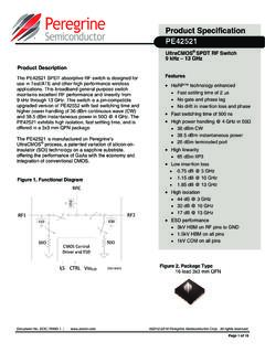
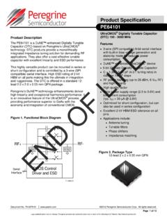
1 Document No. DOC- 13614 -4 Page 1 of 12 2012-2015 Peregrine Semiconductor Corp. All rights reserved. Figure 2. Package Type 32-lead 5 5 mm QFN Product Description The PE42820 is a HaRP technology-enhanced high power reflective SPDT RF switch designed for use in mobile radio, relay replacement and other high performance wireless applications. This switch is a pin-compatible upgraded version of the PE42510A with a wider frequency and power supply range, and external negative supply option. It maintains exceptional linearity and power handling from 30 MHz through GHz. PE42820 also features low insertion loss, high power handling, and is offered in a 32-lead 5 5 mm QFN package. In addition, no external blocking capacitors are required if 0 VDC is present on the RF ports. The PE42820 is manufactured on Peregrine s UltraCMOS process, a patented variation of silicon-on-insulator (SOI) technology on a sapphire substrate.
2 Peregrine s HaRP technology enhancements deliver high linearity and excellent harmonics performance. It is an innovative feature of the UltraCMOS process, offering the performance of GaAs with the economy and integration of conventional CMOS. Product Specification Figure 1. Functional Diagram PE42820 Features High power handling 45 dBm @ 850 MHz, 32W 44 dBm @ 2 GHz, 25W Exceptional linearity 85 dBm IIP3 @ 850 MHz 81 dBm IIP3 @ GHz Low insertion loss dB @ 850 MHz dB @ 2 GHz Wide supply range of + control logic compatible ESD performance kV HBM on all pins External negative supply option DOC-52312 UltraCMOS SPDT RF Switch 30 2700 MHz Product Specification PE42820 Page 2 of 12 2012-2015 Peregrine Semiconductor Corp. All rights reserved. Document No. DOC- 13614 -4 UltraCMOS RFIC Solutions Table 1. Electrical Specifications @ +25 C (ZS = ZL = 50 ), unless otherwise noted Normal mode1: VDD = , VSS_EXT = 0V or Bypass mode2.
3 VDD = , VSS_EXT = Parameter Path Condition Min Typ Max Unit Insertion loss3 RFC RFX 30 MHz 1 GHz dB 1 2 GHz dB 2 GHz dB Isolation RFX RFX 30 MHz 1 GHz 34 35 dB 1 2 GHz 27 28 dB 2 GHz 23 24 dB Unbiased isolation RFC RFX VDD, V1 = 0V, +27 dBm 6 dB Return loss3 RFX 30 MHz 1 GHz 22 dB 1 2 GHz 20 dB 2 GHz 14 dB Harmonics RFC RFX 2fo: +45 dBm pulsed @ 1 GHz, 50 3fo: +45 dBm pulsed @ 1 GHz, 50 94 90 dBc 84 80 dBc Input IP3 RFC RFX 850 MHz 2700 MHz 85 dBm 81 dBm Input compression point4 RFC RFX 30 MHz 2 GHz 2 GHz dBm dBm Switching time 50% CTRL to 90% or 10% RF 15 25 s Settling time 50% CTRL to harmonics within specifications5 30 45 s Notes: 1.
4 Normal mode: single external positive supply used. 2. Bypass mode: both external positive supply and external negative supply used. 3. Performance specified with external matching. Refer to Evaluation Kit section for additional information. 4. The input compression point is a linearity figure of merit. Refer to Table 3 for the operating RF input power (50 ). 5. See harmonics specs above. Product Specification PE42820 Page 3 of 12 Document No. DOC13614-4 2012-2015 Peregrine Semiconductor Corp. All rights reserved. Table 2. Pin Descriptions Table 3. Operating Ranges Figure 3. Pin Configuration (Top View) Pin # Pin Name Description 1, 3 11, 14, 15, 17 22, 24 27, 29 32 GND Ground 2 RF11 RF port 12 VDD Supply voltage (nominal ) 16 VSS_EXT2 External VSS negative voltage control 23 RF21 RF port 28 RFC1 RF common Pad GND Exposed pad.
5 Ground for proper operation 13 V1 Digital control logic input 1 Parameter Symbol Min Typ Max Unit Normal mode1 Supply voltage VDD V Supply current IDD 130 200 A Bypass mode2 Supply voltage VDD V Supply current IDD 50 80 A Negative supply voltage VSS_EXT V Negative supply current ISS 40 16 A Digital input high (V1) VIH V Digital input low (V1) VIL V RF input power, CW 30 MHz 2 GHz >2 GHz PMAX,CW 43 42 dBm dBm RF input power, pulsed4 30 MHz 2 GHz >2 GHz PMAX,PULSED 45 44 dBm dBm RF input power, unbiased PMAX,UNB 27 dBm Operating temperature range (Case) TOP 40 +85 C Operating junction temperature TJ +140 C Normal or Bypass mode Notes: 1.
6 Normal mode: connect pin 16 to GND to enable internal negative voltage generator. 2. Bypass mode: apply a negative voltage to VSS_EXT (pin 16) to bypass and disable internal negative voltage generator. 3. Maximum VIH voltage is limited to VDD and cannot exceed 4. Pulsed, 10% duty cycle of 4620 s period, 50 . 242322212019181712345678 GNDRF1 GNDGNDGNDGNDGNDGNDGNDRF2 GNDGNDGNDGNDGNDGNDE xposed Ground PadPin 1 Dot MarkingNotes: 1. RF pins 2, 23 and 28 must be at 0 VDC. The RF pins do not require DC blocking capacitors for proper operation if the 0 VDC requirement is met. 2. Use VSS_EXT (pin 16, VSS_EXT = VDD) to bypass and disable internal negative voltage generator. Connect VSS_EXT (pin 16, VSS_EXT = GND) to enable internal negative voltage generator. Product Specification PE42820 Page 4 of 12 2012-2015 Peregrine Semiconductor Corp.
7 All rights reserved. Document No. DOC- 13614 -4 UltraCMOS RFIC Solutions Electrostatic Discharge (ESD) Precautions When handling this UltraCMOS device, observe the same precautions that you would use with other ESD-sensitive devices. Although this device contains circuitry to protect it from damage due to ESD, precautions should be taken to avoid exceeding the rating specified. Latch-Up Avoidance Unlike conventional CMOS devices, UltraCMOS devices are immune to latch-up. Table 5. Control Logic Truth Table Path CTRL RFC RF1 H RFC RF2 L Moisture Sensitivity Level The Moisture Sensitivity Level rating for the 32-lead 5 5 mm QFN package is MSL3.
8 Table 4. Absolute Maximum Ratings Exceeding absolute maximum ratings may cause permanent damage. Operation should be restricted to the limits in the Operating Ranges table. Operation between operating range maximum and absolute maximum for extended periods may reduce reliability. Parameter/Condition Symbol Min Max Unit Supply voltage VDD V Digital input voltage (V1) VCTRL V Maximum input power 30 MHz 2 GHz >2 GHz PMAX,ABS dBm dBm Storage temperature range TST 65 +150 C Maximum case temperature TCASE +85 C Peak maximum junction temperature (10 seconds max) TJ +200 C ESD voltage HBM1, all pins VESD 1500 V ESD Voltage MM2, all pins VESD 200 V Notes: 1. Human Body Model (MIL-STD 883 Method 3015).
9 2. Machine Model (JEDEC JESD22-A115). Switching Frequency The PE42820 has a maximum 25 kHz switching rate in normal mode (pin 16 = GND). A faster switching rate is available in bypass mode (pin 16 = VSS_EXT). The rate at which the PE42820 can be switched is then limited to the switching time as specified in Table 1. Switching frequency describes the time duration between switching events. Switching time is the time duration between the point the control signal reaches 50% of the final value and the point the output signal reaches within 10% or 90% of its target value. Spurious Performance The typical low-frequency spurious performance of the PE42820 in normal mode is 137 dBm (pin 16 = GND). If spur-free performance is desired, the internal negative voltage generator can be disabled by applying a negative voltage to VssEXT (pin 16). Optional External VSS Control (VSS_EXT) For applications that require a faster switching rate or spur-free performance, this part can be operated in bypass mode.
10 Bypass mode requires an external negative voltage in addition to an external VDD supply voltage. As specified in Table 3, the external negative voltage (VSS_EXT) when applied to pin 16 will disable and bypass the internal negative voltage generator. Hot Switching Capability The typical hot switching capability of the PE42820 is +30 dBm. Hot switching occurs when RF power is applied while switching between RF ports. Product Specification PE42820 Page 5 of 12 Document No. DOC13614-4 2012-2015 Peregrine Semiconductor Corp. All rights reserved. Typical Performance Data @ +25 C, VDD = , VSS_EXT = 0V, unless otherwise noted Figure 4. Insertion Loss vs. Temp (RFC RFX) Figure 5. Insertion Loss vs. VDD (RFC RFX) Figure 6. RFC Port Return Loss vs. Temp (RF1 Active) Figure 7. RFC Port Return Loss vs. VDD (RF1 Active) Product Specification PE42820 Page 6 of 12 2012-2015 Peregrine Semiconductor Corp.