Transcription of Product Specification PE64906 - psemi.com
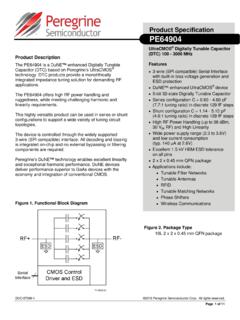
1 Page 1 of 11 Document No. DOC-82123-3 2017 Peregrine Semiconductor Corp. All rights reserved. PE64906 is a DuNE technology-enhanced digitally tunable capacitor (DTC) based on Peregrine s UltraCMOS technology. This highly versatile Product supports a wide variety of tuning circuit topologies with emphasis on impedance matching and aperture tuning applications. PE64906 offers high RF power handling and ruggedness while meeting challenging harmonic and linearity requirements enabled by Peregrine s HaRP technology. The device is controlled through the widely supported 3-wire (SPI compatible) interface.
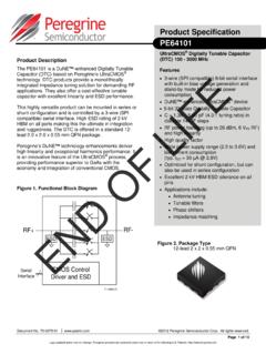
2 All decoding and biasing is integrated on-chip and no external bypassing or filtering components are required. DuNE devices feature ease of use while delivering superior RF performance in the form of tuning accuracy, monotonicity, tuning ratio, power handling, size, and quality factor. With built-in bias voltage generation and ESD protection, DTC products provide a monolithically integrated tuning solution for demanding RF applications. Product Specification Product Description Figure 1. Functional Diagram Figure 2. Package Type 10-lead 2 x 2 x mm QFN CMOS Control Driver and ESDRF+RF-Serial InterfaceESDESDU ltraCMOS Digitally Tunable Capacitor (DTC) 100 - 3000 MHz PE64906 Features 3-wire (SPI compatible) serial interface with built-in bias voltage generation and ESD protection DuNE technology enhanced 5-bit 32-state digitally tunable capacitor Shunt configuration C = pF to pF ( :1 tuning ratio) in discrete 119 fF steps High RF power handling (30 Vpk RF) and linearity Wide power supply range ( to ) and low current consumption (typ.)
3 140 A at ) High ESD tolerance of 2 kV HBM on all pins Applications include: Tunable antennas Tunable matching networks Tunable filter networks Phase shifters DOC-02169 Page 2 of 11 2017 Peregrine Semiconductor Corp. All rights reserved. Document No. DOC-82123-3 UltraCMOS RFIC Solutions Product Specification PE64906 Table 1. Electrical Specifications @ 25 C, VDD = (In shunt configuration, RF- connected to GND) Parameter Condition Min Typ Max Unit Operating frequency 100 3000
4 MHz Minimum capacitance (Cmin) State = 00000, 100 MHz pF Maximum capacitance (Cmax) State = 11111, 100 MHz pF Tuning ratio Cmax/Cmin, 100 MHz :1 Step size 5 bits (32 states), 100 MHz pF Quality factor at Cmin1 698 960 MHz, with LS removed 1710 2170 MHz, with LS removed 40 40 Quality factor at Cmax1 698 960 MHz, with LS removed 1710 2170 MHz, with LS removed 29 13 Self resonant frequency State 00000 State 11111 GHz Harmonics2 2fo, 3fo: 698 915 MHz; PIN = +34 dBm, 50 2fo, 3fo: 1710 1910 MHz; PIN = +32 dBm, 50 36 36 dBm dBm IMD3 Bands I,II,V/VIII, +20 dBm CW @ TX freq, 15 dBm CW @ 2TX-RX freq, 50 105 dBm Switching time3,4 State change to 10/90% delta capacitance between any two states 12 s Start-up time3 Time from VDD within Specification to all performances within Specification 70 s Wake-up time3,4 State change from Standby mode to RF state to all performances within Specification 70 s Third order intercept point (IP3) Shunt configuration derived from IMD3 spec IP3 = (2 PTX + Pblock IMD3)
5 / 2 65 dBm Notes: 1. Q for a shunt DTC based on a series RLC equivalent circuit Q = XC / R = (X - XL) / R, where X = XL + XC , XL = 2*pi*f*L, XC = -1 / (2*pi*f*C), which is equal to removing the effect of parasitic inductance LS 2. In shunt between 50 ports. Pulsed RF input with 4620 S period, 50% duty cycle, measured per 3 GPP TS 3. DC path to ground at RF must be provided to achieve specified performance 4. State change activated on falling edge of SEN following data word Page 3 of 11 Document No.
6 DOC-82123-3 2017 Peregrine Semiconductor Corp. All rights reserved. Product Specification PE64906 Pin # Pin Name Description 1 RF- Negative RF port1 2 RF- Negative RF port1 3 GND Ground2 4 VDD Power supply pin 5 SCL Serial interface clock input 6 SEN Serial interface latch enable input 7 SDA Serial interface data input 8 RF+ Positive RF port1 9 RF+ Positive RF port1 10 GND Ground2 Pad GND Exposed pad: ground for proper operation2 Table 3.
7 Operating Ranges Parameter Min Typ Max Unit Supply voltage V Supply current (VDD = ) 140 200 A Digital input high V Digital input low 0 0 V Peak operating RF voltage2 VP to VM VP to RFGND 30 30 Vpk Vpk Operating temperature range 40 +25 +85 C Storage temperature range 65 +25 +150 C Standby current (VDD = ) 25 A RF input power (50 )1 698 915 MHz 1710 1910 MHz +34 +32 dBm dBm Symbol VDD IDD IDD VIH VIL TOP TST Figure 3. Pin Configuration (Top View) Table 2.
8 Pin Descriptions Exceeding absolute maximum ratings may cause permanent damage. Operation should be restricted to the limits in the Operating Ranges table. Operation between operating range maximum and absolute maximum for extended periods may reduce reliability. Table 4. Absolute Maximum Ratings Parameter/Condition Symbol Min Max Unit ESD Voltage HBM* VESD 2000 V Latch-Up Avoidance Unlike conventional CMOS devices, UltraCMOS devices are immune to latch-up. Electrostatic Discharge (ESD) Precautions When handling this UltraCMOS device, observe the same precautions that you would use with other ESD-sensitive devices.
9 Although this device contains circuitry to protect it from damage due to ESD, precautions should be taken to avoid exceeding the specified rating. Moisture Sensitivity Level The Moisture Sensitivity Level rating for the PE64906 in the 10-lead 2 x 2 x mm QFN package is MSL1. Notes: 1. Maximum power available from 50 source. Pulsed RF input with 4620 S period, 50% duty cycle, measured per 3 GPP TS measured in shunt between 50 ports, RF- connected to GND 2. Node voltages defined per Equivalent Circuit Model Schematic (Figure 13). When DTC is used as a part of reactive network, impedance transformation may cause the internal RF voltages (VP, VM) to exceed peak operating RF voltage even with specified RF input power levels.
10 For operation above about +20 dBm (100 mW), the complete RF circuit must be simulated using actual input power and load conditions, and internal node voltages (VP, VM in Figure 13) monitored to not exceed 30 Vpk Notes: 1. For optimal performance, recommend tying Pins 1-2 and Pins 8-9 together on PCB 2. For optimal performance, recommend tying Pins 3, 10 and exposed ground pad together on PCB Note: * Human Body Model (MIL-STD-883 Method ) Page 4 of 11 2017 Peregrine Semiconductor Corp. All rights reserved. Document No. DOC-82123-3 UltraCMOS RFIC Solutions Product Specification PE64906 Frequency(800 - 900 MHz)C0C1C2C4C8C15C31 Figure 5.