Transcription of Radiofrequency Plasma Sources for Semiconductor Processing
1 1234567891011121314151617181920212223242 5262728293031323334353637383940414243444 5 Druckfreigabe/approvalforprintingWithout corrections/`ohneKorrekturenAftercorrect ions/nachAusf hrung`derKorrekturenDate/Datum:..Signatu re/Zeichen:..6 Radiofrequency Plasma Sources for Semiconductor ProcessingFrancis F. the etching and deposition steps in the production of Semiconductor chips, plasmaprocessing is required for three main reasons. First, electrons are used to dissociatethe input gas into atoms. Second, the etch rate is greatly enhanced by ion bombard-ment, which breaks the bonds in the first few monolayers of the surface, allowing theetchant atoms, usually Cl or F, to combine with substrate atoms to form volatilemolecules.
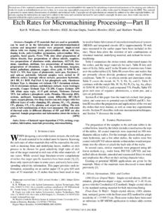
2 And third, most importantly, the electric field of the Plasma sheathstraightens the orbits of the bombarding ions so that the etching is anisotropic,allowing the creation of features approaching nanometer Plasma Sources used in the Semiconductor industry were originally developedby trial and error, with little basic understanding of how they work. To achieve thisunderstanding, many challenging physics problems had to be solved. This chapter isan introduction to the science of Radiofrequency (rf ) Plasma Sources , which are by farthe most common. Sources operating at zero or other frequencies, such as GHzmicrowaves, lie outside our scope. Most rf Sources use the MHz industrialstandard frequency. Among these, there are three main types: (1) capacitively coupledplasmas or CCPs, also called reactive ion etchers (RIEs); (2) inductively coupledplasmas (ICPs), also called transformer coupled plasmas (TCPs); and (3) heliconwave Sources , which are new and can be called Coupled PlasmasThe principal parts of a CCPare shown schematically in Fig.
3 In its simplest form,the rfvoltageisappliedacrosstwoparallelmetal plates,generatinganoscillatingelectricfi eld between them. This field accelerates electrons, heating their thermal distributionto have enough high-energy electrons in the tail to cause an ionization avalanche. silicon wafer to be processed is attached to the normally grounded electrode by anAdvanced Plasma Technology. Edited by Riccardo d Agostino, Pietro Favia, Yoshinobu Kawai, Hideo Ikegami,Noriyoshi Sato, and Farzaneh Arefi-KhonsariCopyright 2007 WILEY-VCH Verlag GmbH & Co. KGaA, WeinheimISBN: electrode and also provides small channels for flow of helium to cool the wafer. Tokeeptheplasmaneutral,sheathsautomatica llyformnexttotheelectrodesprovidinganele ctric field (E-field) perpendicular to their surfaces.
4 The potential drop in the sheathrepels the fast-moving electrons so that they can escape no faster than the ions. At thesame time, the sheath E-field accelerates the ions to bombard the surface and performthe beneficial functions mentioned sheath drop is of order 5 KTe, whereTeis the electron temperature. For a 3 eVplasma, the ion energy is of order 15 eV. Since rf voltage is applied, the sheath dropand sheath thickness will oscillate at the rf frequency. Even if one electrode isgrounded, the Plasma potential will oscillate so as to make the two sheaths identical,but out of phase. The sheath oscillation will affect the ionenergy distribution function(IEDF), depending on the transit time of the ions through the sheath.
5 At lowpressures, the IEDF at the wafer surface tends to be bimodal, with peaks at themaximum and minimum sheath drops, since a sine wave changes slowly at itsextrema. CCPs are relatively inefficient ionizers and work best at high pressures andlow densities. The sheath thickness, therefore, can become measurably large, oforder millimeters. If the ion mean free path (mfp) for collisions with neutrals issmaller than the sheath thickness, the IEDF will be pressure-broadened. There arealso other heating mechanisms. In resonant heating, some fast electrons can travelbetween the two sheaths without colliding, and those with just the right velocity cancatch each sheath in its expanding phase, thus getting accelerated at each effects in classic CCPs are further described in textbooks [1,2].
6 CCPsIf ion bombardment energies larger than the normal sheath drop are desired, onecan apply a second rf source, abias oscillator, to the electrode bearing the of a capacitive Radiofrequency Plasma Sources for Semiconductor Processing123456789101112131415161718192 0212223242526272829303132333435363738394 04142434445 This is usually at a lower frequency, which has a larger effect on the massive ions. Thetime-averaged sheath drop will then increase by the following rectification the electrode is driven positive, a large electron current flows to it through thelowered Coulomb barrier, but when the electrode goes negative, there is nocorresponding ion current because the ions are much slower. Unless the electrodeemits electrons, it will accumulate a negative charge.
7 Applying a large rf bias voltageto the substrate will, therefore, increase the dc (direct current) sheath drop eventhough the bias voltage is ac. It is not generally possible to apply a dc voltage directly,since parts of the wafer may be non-conducting. An rf voltage, however, will beconveyed capacitively through these insulating power supplies have been used for many years, but recently the dual-frequency concept has found an important application in CCPs with extremely thingaps. These new devices perform well in oxide etch; that is, in the etching of SiO2,adifficult process since Si intrinsically etches faster than its oxide. The reason that thin-gap CCPs work is not yet understood, but interest in them has spawned computa-tional studies which have advanced the science of CCPs in general.
8 Figure shows aschematic of this type of source. The electrodes are asymmetric; the wafer-bearingplate is smaller to enhance the sheath drop there. The high frequency produces theplasma, and the low frequency controls the ion distribution in the sheath. Thesedevices are quite different from the original RIEs because they operate at highpressure (10 100 mtorr), and the gaps are very small (1 3 cm). With high rf biasvoltage, the sheaths are quite thick and can occupy most of the volume, leaving only asmall region of quasineutral Plasma near the midplane. In this limit, what happens inthe sheath controls the Plasma production. Upon striking the substrate, thoseelectrons that have penetrated the sheath produce more electrons by secondaryemission.
9 The emitted electrons are then accelerated toward the Plasma by the sheathfield. They ionize the neutral gas inside the sheath, since the ionization mfp can besmaller than the sheath thickness. The avalanche that creates the Plasma then startsin the the sheaths oscillate at two frequencies and their beats and harmonics, it isclear that extensive computer simulation is required to model the complicatedFig. of a thin-gap, dual-frequency Capacitively Coupled Plasmas101123456789101112131415161718192 0212223242526272829303132333435363738394 04142434445behavior in these collisional sheaths. We quote here just a few results from Lee sgroup at Pohang University in South Korea [3,5]. It is well known [1] in CCPs that thedensity increases with the square of the frequency.
10 At constant power, therefore, thedensity increases, and the Debye length decreases, with frequency. The resultingchange in sheath thickness is clearly demonstrated in Fig. The IEDFs and EEDF schange not only with frequency but also with pressure. The pressure variation ofIEDF is shown in Fig. , where it is seen that the typical bimodal distribution at lowpressure is smoothed out by collisions at high pressure. Particle-in-cell simulationsare invaluable in understanding complicated plasmas such as these. However, someaspects, such as why CCPs create less damage to oxide layers in etching, are stillbeyond the capabilities of theory. At this point, CCPs have been revived both asimportant manufacturing tools and as academically interesting of ion and electron density profiles at variousfrequencies [5].