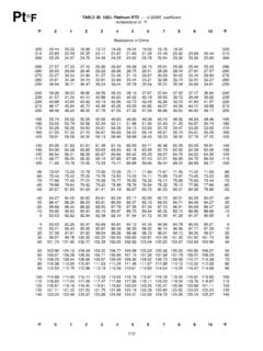
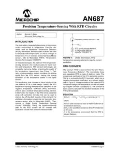
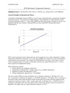
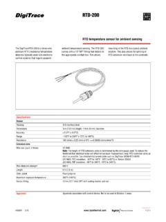
Transcription of rtd circuits - kennethkuhn.com
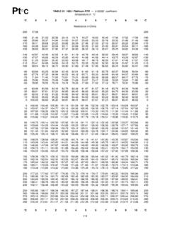
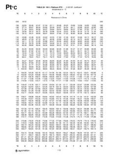
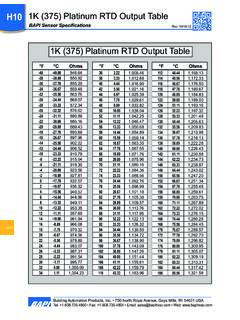
1 RTD Circuits1by Kenneth A. KuhnMarch 19, 2011, rev. March 28, 2011 IntroductionThe abbreviation, RTD, refers to a resistor that has a predictable increase in resistancewith temperature. There are a variety of interpretations of RTD ResistanceThermometer Device, Resistance Temperature Detector, etc. All refer to the same most common RTD is made of pure Platinum wire and has a resistance of at 0 C. RTDs are known by their resistance at 0 C. At lower temperatures thechange in resistance with temperature is fairly constant at about ohms per C. Athigher temperatures the change becomes less and non-linear correction is needed that isbeyond the scope of this note. For simplicity we will consider the device to be values of RTD 0 C resistances are available from a few tens of ohms to tenthousand ohms. A 10K RTD would have a resistance change per C of 39 ohms.
2 Copperwire can also be used as an RTD and has similar characteristics to Platinum up to around100 C. Above that temperature Copper tends to degrade and also has a more non-linearresponse. As an example, if the resistance of a 100 ohm rtd was 130 ohms then thetemperature would be (130 100) / = 77 RTD is normally operated with a small constant current (typically between about 100uA and 1 mA for a 100 ohm device) so that the response is linear. The current must besmall enough so that heating effects are negligibly small. The voltage across the RTD isthen the voltage at 0 C resulting from the constant current times the 0 C resistance plusthe change in resistance times the constant current. This is not unlike a semiconductordiode characteristic except that the slope is positive instead of negative. RTD processinginvolves scaling the change in resistance to a change in voltage (often 10 mV / C) andremoving the 0 C offset.
3 There are a variety of circuits to do are often located a distance (perhaps many tens of feet) from the processingelectronics. The resistance of the connecting wires adds to that of the RTD and is anerror term. The 4-wire Kelvin connection eliminates the error. A modified 3-wire Kelvinconnection is most commonly used. Two methods for doing this are illustrated in thefollowing 1 The RTD processing circuit in Figure 1 illustrates a simplistic method based on simplecircuits that students should know. Although the circuit works fine, it uses a lot of circuits will use more advanced concepts and fewer parts. This circuit isexcellent for students to use as a learning Circuits2 RTDRw1Rw2Rw3R1R2R3R4R5R6R7R8R9U1U2U3-VRV oCircuit 1 The circuit requires a negative reference voltage (typically , , , or ).U1 is an inverting amplifier with the RTD in the feedback path.
4 The constant currentthrough the RTD is the voltage reference divided by R1. This current is typically in therange of 100 uA to 1 mA for a 100 ohm rtd . For this example we will use VR = and R1 = 10K so that the constant current through a 100 ohm rtd is 500 uA. Allof the Rw wire resistances are identical the numbers are an aid in discussing a particularresistance. The current through the RTD passes through Rw1 and Rw3. There is nocurrent (technically, it is negligibly small) in Rw2. The voltage at the R2 input is the sumof the RTD voltage and the voltage drop across two connecting wires in series. Thevoltage at the R4 input is the voltage drop across Rw3. All we need to do is to subtracttwice the voltage at the R4 input from the voltage at the R2 input and the effect of voltagedrop in the wires connecting the RTD will vanish at the output of U2.
5 We need forR5/R4 to be two but this will make the non-inverting gain equal to three and we need thatgain to be one. Thus, we include a voltage divider, R2 and R3, that has a transfer gain ofone-third so that the net non-inverting gain of U2 is one and its output voltage is thevoltage across the RTD. One set of resistors that will accomplish this is R2 = 200K, R3= 100K, R4 = 100K, and R5 = next step is to remove the offset voltage at 0 C and this is done with the voltagedivider formed by R6 and R7. At 0 C the output of U2 is the constant current multipliedby the RTD resistance 500 uA * 100 ohms = volts. The desired voltage at the non-inverting input to U3 is zero volts. We can choose R6 to be any convenient value wewill choose 1K and the current through R6 will be / 1K = 50 uA. R7 will have (0 --VR) or 5 volts across it and should conduct 50 uA.
6 R7 calculates to be last step is to determine R8 and R9 for the desired output scale factor we want 10mV / C. The 100 RTD will increase by ohms per C which becomes 195 uV / Cwhen multiplied by the 500 uA constant current. The voltage division by R6 and R7reduces this to uV / C. Thus, the non-inverting gain of U3 must be /RTD = This means that R9/R8 = We could choose R8 = 1K andthen R9 will be the example with R1 modified so that the constant current is 1 problem 1 with the reference voltage changed to volts. Try theother common reference voltages a test you would be given the RTD value, VR, and probably R2 through would also be given either R6 or R7 and either R8 or R9 and the desiredoutput scale factor. Your job would be to calculate the value of the resistors 2 circuit 2 is the same concept as that of circuit 1 except that the reference wire on theRTD is to the high side rather than to the ground side.
7 Although using the ground sideseems more intuitive, the circuitry for processing the high side is simpler. That is typicalfor a lot of circuits the obvious method takes more parts and a non obvious approachworks the same but with fewer parts. As before, all of the Rw resistances are identical the numbers are only so that a specific resistance can be 2 Note that the RTD system is in the feedback of U1 and that the current is VR / R1. Thiscurrent would typically be in the range of 100 uA to 1 mA for a 100 ohm rtd . Thevoltage at the output of U1 is VRTD + 2*Vw (the current is through Rw1 and Rw3). Thevoltage at the non-inverting input to U2 is VRTD + Vw (there is no current throughRTD Circuits4Rw2). R2 and R3 are the same value (perhaps 10K). The output of U2 is then 2*(VRTD+ Vw) (VRTD + 2*Vw) = VRTD.
8 For this example we will use a 100 ohm rtd andVR = volts, and R1 = 10K so that the constant current is 500 uA. The studentshould carefully work the math regarding U2 to fully understand the next step is to remove the offset voltage at 0 C and this is done with the voltagedivider formed by R4 and R5. At 0 C the output of U2 is the constant current multipliedby the RTD resistance 500 uA * 100 ohms = volts. The desired voltage at the non-inverting input to U3 is zero volts. We can choose R4 to be any convenient value wewill choose 1K and the current through R5 will be / 1K = 50 uA. R5 will have (0 --VR) or 5 volts across it and should conduct 50 uA. R5 calculates to be last step is to determine R6 and R7 for the desired output scale factor we want 10mV / C. The 100 RTD will increase by ohms per C which becomes 195 uV / Cwhen multiplied by the 500 uA constant current.
9 The voltage division by R4 and R5reduces this to uV / C. Thus, the non-inverting gain of U3 must be = This means that R7/R6 = We could choose R6 = 1K andthen R7 will be the example for VR = , , and volts. Also, change theoutput scale factor for one of the problems to 50 mV /C. For all cases, calculateR1 for a constant current of a test you would be given VR, the desired constant current, either R2 or R3,either R6 or R4, and the desired output scale factor. You would have to calculateR1 and the resistors not 3 The circuit in Figure 3 is much simpler than the previous two although it requires a 4-wire Kelvin connection. It is the result of really thinking about the simplest method toaccomplish what is desired. All Rw resistances are equal the numbers are an aid torefer to a particular resistance.
10 Typical values for Rw range from less than one ohm forshort cables to several ohms for long cables. Point L on the RTD is held at virtual groundby feedback from U1. There is current through Rw4 but no current through Rw3 thusno voltage drop. The current is the reference voltage (typically ) across the sum ofR1 and Rw4 and is typically in the 100 uA to 1 mA range for 100 ohm RTDs. Feedbackcurrent from U1 is through Rw2 and the RTD. Thus, ignoring a tiny voltage drop acrossRW1, the voltage across R3 is the RTD voltage and this is a negative voltage becauseof the inverting amplifier. R2 is calculated to sum current into the virtual ground of U2so that there is no feedback current through R4 when the RTD is at 0 C. R4 is calculatedto provide the desired output scale Circuits5Rw1Rw2Rw3Rw4 VoR1R2R3R4U1U2 RTDVRLHF igure 3:As an example, If VR is volts and R1 is 10K then the current is 500 uA and thevoltage across the RTD is then -500 uA*(100 + *T) or - *T volts.