Transcription of SCDS330C - Texas Instruments
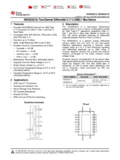
1 Primary HDMI SourcePrimary SourceDDC & CEC orAux & HPDTS3DV621 DataChannelChannelHDMI ReceiverGraphicProcessorSecondary SourceDDC & CEC orAux & HPDS econdary HDMI orDisplayPort SourceTS3DV621 SidebandVideo JANUARY2012 REVISEDMAY201312-Channel1:2 MUX/DEMUXS witchwithIntegrated4-ChannelSidebandSign alSwitchingforDVI/HDMIandDisplayPort(DP) ApplicationsCheckforSamples:TS3DV6211 FEATURESAPPLICATIONS SwitchType:2:1or1:2 DVI/HDMI/DisplayPortSignalSwitching DataRateCompatibility GeneralPurposeTMDS/LVDSS ignalSwitching :2or2:1bi-directional Bandwidth(-3dB) (DDC,AUX,CEC,orHPD) RON 8 3 ,theTS3DV621offerslowandflatON-stateresi stance CON ,whichallowsthe VCCR ange I/OVoltageRange 0 5 ,DVI,andDisplayPort Bit-to-BitSkew 6 PropagationDelay 40psTypicalphysicallinkinterfacefroma singleHDMI porttotwo SpecialFeaturesHDMI ports(AorB port) canalsobeusedforDisplayPort(DP)source/si nkapplications. DedicatedEnableLogicSupportsHi-ZTheinteg ratedside-bandcontrolchannelsallow5 VModesignalstopassthrough,makingtheTS3DV 621 (VCC= 0 V)ThemostcommonapplicationfortheTS3DV621 is ,therearetwo 2kVHumanBodyModel(A114B,ClassII)possible sources(DVD,set-topbox,orgame 1kVChargedDeviceModel(C101)console) inthehigh-impedancemode,such 42-pinQFNP ackage(9x , ) , (HDMI/ displayport )
2 1 Pleasebeawarethatanimportantnoticeconcer ningavailability,standardwarranty,anduse in 2012 2013, +AD3+AD1 AD3 AD2+AAUX+AD2 AAUX AD1+BD3+BD1 BD3 BD2+BAUX+BD2 BAUX BVCCVCCD0+D0 D1+ENAUX D1 D2+D2 SEL1 SEL2D3+D3 AUX+HPDCECVCCHPDACECBCECAHPDBD0 BD0+BD0+AD0 AGNDTS3DV621 SCDS330C JANUARY2012 ,17,30 PowerSupplyVoltageGNDP owerPadGroundGroundEN8 IEnableInputSEL19 ISelectInput1 SEL210 ISelectInput2D0+A41I/OPortA,Lane0,+vesig nalD0-A39I/OPortA,Lane0,-vesignalD1+A38I /OPortA,Lane1,+vesignalD1-A36I/OPortA,La ne1,-vesignalD2+A34I/OPortA,Lane2,+vesig nalD2-A32I/OPortA,Lane2,-vesignalD3+A29I /OPortA,Lane3,+vesignalD3-A27I/OPortA,La ne3,-vesignalD0+B42I/OPortB,Lane0,+vesig nalD0-B40I/OPortB,Lane0,-vesignalD1+B37I /OPortB,Lane1,+vesignalD1-B35I/OPortB,La ne1,-vesignalD2+B33I/OPortB,Lane2,+vesig nalD2-B31I/OPortB,Lane2,-vesignalD3+B28I /OPortB,Lane3,+vesignalD3-B26I/OPortB,La ne3,-vesignalD0+2I/OCommonPort,Lane0,+ve signalD0 3I/OCommonPort,Lane0,-vesignalD1+4I/OCom monPort,Lane1,+vesignalD1 5I/OCommonPort,Lane1,-vesignalD2+6I/OCom monPort,Lane2,+vesignalD2 7I/OCommonPort,Lane2,-vesignalD3+11I/OCo mmonPort,Lane3,+vesignalD3-12I/OCommonPo rt,Lane3,-vesignalAUX+A25I/O+veAUXC hannelforPortAAUX-A23I/O-veAUXC hannelforPortAHPDA21I/OPortA HPDCECA19I/OPortA CECAUX+B24I/O+veAUXC hannelforPortBAUX-B22I/O-veAUXC hannelforPortBHPDB20I/OPortB HPDCECB18I/OPortB CECAUX+13I/O+veAUXC hannelforCommonPortAUX 14I/O-veAUXC hannelforCommonPortHPD15I/OHPDforCommonP ortCEC16I/OCECforCommonPort2 SubmitDocumentationFeedbackCopyright 2012 2013,TexasInstrumentsIncorporatedProduct FolderLinks.
3 TS3DV621D0+SEL1 Control LogicSEL2 AUX+AUX HPDCECENAUX+AAUX AHPDACECAAUX+BAUX BHPDBCECBD0 D1+D1 D2+D2 D3+D3 D0+AD0 AD1+AD1 AD2+AD2 AD3+AD3 AD0+BD0 BD1+BD1 BD2+BD2 BD3+BD3 JANUARY2012 HighImpedanceOutputportA = InputHL(1)L(1)OutputPortB = HighImpedanceOutputPortA = HighImpedanceHH(1)H(1)OutputPortB = Input(1)TieSEL1andSEL2togetherforeasyout putcontrolCopyright 2012 2013,TexasInstrumentsIncorporatedSubmitD ocumentationFeedback3 ProductFolderLinks:TS3DV621D0+D0-D2+D1-D 1+D3+D2-D3-Cab_DetectAUX/DDCHPDAUX/DDCTS 3DV621DP/HDMIS witchDual ModeDisplayPortSourceDual ModeDisplayPortConnectorHDMIC onnectorD0+D0-D2+D1-D1+D3+D2-D3-Cab _DetectAUX-HPDAUX+D0+D0-D2+D1-D1+D3+D2-D 3-DDC_DATAHPDDDC_CLKD0+D0-D2+D1-D1+D3+D2 -D3-CECDDC DATAHPDDDC CLKTS3DV621 HDMI SwitchHDMIT ransmitter 1 HDMIR eceiverDisplay(DLP, LCD, TV,PDP, HDTV)HDMI Scalar/Video DecoderD0+AD0-AD2+AD1-AD1+AD3+AD2-AD3-AC EC_ADDC DATA _AHPD_ADDC CLK _AHDMIT ransmitter 1D0+BD0-BD2+BD1-BD1+BD3+BD2-BD3-BCEC_BDD C DATA _BHPD_BDDC CLK _BTS3DV621 SCDS330C JANUARY2012 2012 2013, JANUARY2012 REVISEDMAY2013 ABSOLUTEMAXIMUMRATINGS(1)overoperatingfr ee-airtemperaturerange(unlessotherwiseno ted) (2)(3)(4)AllI/O (2)(3)SEL1,SEL2 < 0 50mAIIKD igitalinputclampcurrentVIN< 0 50mAII/OOn-stateswitchcurrent(5)AllI/O 128128mAIDDC ontinuouscurrentthroughVDDorGND 100100mAIGND JAPackagethermalimpedance(6) C/WTstgStoragetemperaturerange 65150 C(1)
4 Stressesbeyondthoselistedunder"AbsoluteM aximumRatings" recommendedoperatingconditions is (2)Allvoltagesarewithrespecttoground,unl essotherwisespecified.(3)Theinputandoutp utvoltageratingsmaybeexceededif theinputandoutputclamp-currentratingsare observed.(4)VIandVOareusedtodenotespecif icconditionsforVI/O.(5)IIandIOareusedtod enotespecificconditionsforII/O.(6)Thepac kagethermalimpedanceis calculatedin accordancewithJESD51-7 RECOMMENDEDOPERATINGCONDITIONS(1) , , , 4085 C(1) ,ImplicationsofSloworFloatingCMOSI nputs, 2012 2013,TexasInstrumentsIncorporatedSubmitD ocumentationFeedback5 ProductFolderLinks:TS3DV621TS3DV621 SCDS330C JANUARY2012 (1)MINTYP(2)MAXUNITVIKD igitalinputclampvoltageSEL1,SEL2 VCC= ,IIN= -18mA 3 V, VI/O VCC, II/O= 40mA812 VCC= 3 V,VI/O= andVCC,RON(flat)(3)On- II/O= 40mAOn-stateresistancematch RON(4)AllI/OVCC= 3 V, VI/O VCC, II/O= betweenchannelsDigitalinputhighleakageII HSEL1,SEL2 VCC= , VIN= VDD 1 AcurrentDigitalinputlowleakageIILSEL1,SE L2 VCC= ,VIN= GND 1 AcurrentLeakageunderpoweroffIOFFA lloutputsVCC= 0 V,VI/O= 0 ,VIN= 0 1 AconditionsCIND igitalinputcapacitanceSEL1,SEL2f = 1 MHz,VIN= 0 = 1 MHz,VI/O= 0 V,Outputis open,COFFS witchOFFcapacitanceAllI/O2pFSwitchis OFFf = 1 MHz,VI/O= 0 V,Outputis open, ONICCVCC supplycurrentVCC= ,II/O= 0,VIN= VDDorGND300400 A(1)VI, VO, II, andIOrefertoI/Opins,VINreferstothecontro linputs(2)AlltypicalvaluesareatVCC= (unlessotherwisenoted),TA= 25 C(3)RON(FLAT)is thedifferenceofRONin a givenchannelatspecifiedvoltages.
5 (4) RONis ,VCC= ,RL= 200 , CL= 4 pF(unlessotherwisenoted)(seeand)FROMTOPA RAMETERMINTYP(1)MAXUNIT(INPUT)(OUTPUT)tp d(2)AllI/OinputsideAllI/Ooutputside40pst PZH, tPZLSEL1,SEL2 AllI/O27nstPHZ, tPLZSEL1,SEL2 AllI/O25nstsk(o)(3)AllI/OinputsideAllI/O outputside630pstsk(p)(4)630ps(1)Alltypic alvaluesareatVCC= (unlessotherwisenoted),TA= 25 C.(2)Thepropagationdelayis thecalculatedRCtimeconstantofthetypicalO N-Stateresistanceoftheswitchandthespecif iedloadcapacitancewhendrivenbyanidealvol tagesource(zerooutputimpedance).(3)Outpu tskewbetweencenterportandanyotherchannel .(4)Skewbetweenoppositetransitionsofthes ameoutput|tPHL tPLH|DYNAMICCHARACTERISTICSO verrecommendedoperationfree-airtemperatu rerange,VCC= (unlessotherwisenoted)PARAMETERTESTCONDI TIONSTYP(1)UNITXTALKRL= 50 , f = 250 MHz(Figure11) 43dBOIRRRL= 50 , f = 250 MHz(Figure12) 42dBBWRL= 50 , SwitchON(Figure10) (1)AlltypicalvaluesareatVCC= (unlessotherwisenoted),TA= 25 2012 2013, +05 +06 +07 +08 +09 +10f - Frequency - HzAttenuation - dBR-ONWV - Input Voltage - +05 +06 +07 +08 +09 +10f - Frequency - HzAttenuation - +05 +06 +07 +08 +09 +10f - Frequency - HzAttenuation - JANUARY2012 2012 2013,TexasInstrumentsIncorporatedSubmitD ocumentationFeedback7 ProductFolderLinks:TS3DV621CL(see Note A)TEST CIRCUITS12 VDDOpenGNDRLRLNOTES: A.
6 CLincludes probe and jig Waveform 1 is for an output with internal conditions such that the output is low, except when disabled by the output 2 is for an output with internal conditions such that the output is high, except when disabled by the output input pulses are supplied by generators having the following characteristics:PRR 10 MHz, ZO= 50 , tr ns, tf The outputs are measured one at a time, with one transition per tPLZand tPHZare the same as tPZLand tPZHare the same as VG1 VDDDUT50 VIN50 VG250 VITESTRLS1V CLVDDVintPLZ/tPZL2 VDD200 GND4 VInput GeneratorInput GeneratorVOtPHZ/tPZHGND200 VDD4 VtPZLVOH- VVOLTAGE WAVEFORMSENABLE AND DISABLE TIMESVCC/2 VDC/2 Output Control(VIN)VOHVOL+ VVOHVOL0 VtPZHtPLZtPHZO utputWaveform 2S1 at GND(see Note B)OutputWaveform 1S1 at 2 x VCC(see Note B) V V VTS3DV621 SCDS330C JANUARY2012 2012 2013,TexasInstrumentsIncorporatedProduct FolderLinks:TS3DV621CL(see Note A)TEST CIRCUITS12 VDDOpenGNDRLRLVOHVOLVOLTAGE WAVEFORMSOUTPUT SKEW (tsk(o))Data Out atYB1or YB2 NOTES: A.
7 CLincludes probe and jig Waveform 1 is for an output with internal conditions such that the output is low, except when disabled by the output 2 is for an output with internal conditions such that the output is high, except when disabled by the output All input pulses are supplied by generators having the following characteristics: PRR 10 MHz, ZO= 50 , tr ns, tf The outputs are measured one at a time, with one transition per VG1 VDDDUT50 VSEL50 VG250 VIInput GeneratorInput GeneratorVO(VOH+ VOL)/2 VOHVOLData Out atXB1or XB2(VOH+ VOL) VData In atAx or AytPLHxtPHLxtsk(o)tsk(o)tPLHytPHLytsk(o) = tPLHy tPLHxor tPHLy tPHLxVOHVOLVOLTAGE WAVEFORMSPULSE SKEW [tsk(p)]Output(VOH+ VOL)/2 InputtPLHtPHLtsk(p)= tPHL V VVCCV intsk(p)tsk(o) V VCCor GNDVCCor GND4 pF4 pF200 JANUARY2012 REVISEDMAY2013 PARAMETERMEASUREMENTINFORMATION(continue d) 2012 2013,TexasInstrumentsIncorporatedSubmitD ocumentationFeedback9 ProductFolderLinks:TS3DV621 EXT TRIGGERBIASN etwork Analyzer(HP8753ES)P1P2 VCCAXBXSELDUTVBIASVSELTS3DV621 SCDS330C JANUARY2012 (continued) (BW)Frequencyresponseis ,whenVSEL= 0 andA0is theinput,theoutputis 4 RBW= 3 kHzVBIAS= 2 sP1= 0 dBM10 SubmitDocumentationFeedbackCopyright 2012 2013,TexasInstrumentsIncorporatedProduct FolderLinks:TS3DV621 VSELA.
8 C includes probe and jig A 50 W termination resistor is needed to match the loading of the network TRIGGERBIASN etwork Analyzer(HP8753ES)P1P2A0A1A2A3 SELBXBXBXBXBXBXBXBXVCCR = 50 LWR = JANUARY2012 REVISEDMAY2013 PARAMETERMEASUREMENTINFORMATION(continue d) (XTALK)Crosstalkis ,whenVSEL= 0 andA1is theinput,theoutputismeasuredatA3. Allunusedanaloginput(A)portsareconnected toGND,andoutput(B) 4 RBW= 3 kHzVBIAS= 2 sP1= 0 dBMCopyright 2012 2013,TexasInstrumentsIncorporatedSubmitD ocumentationFeedback11 ProductFolderLinks:TS3DV621 VDDA00B1 SELDUTVBIASVSELEXT TRIGGERBIASN etwork Analyzer(HP8753ES)P1P2A11B10B21BX2R = 50 LWA. C includes probe and jig A 50 W termination resistor is needed to match the loading of the network JANUARY2012 (continued) (OIRR)OFFisolationis ,whenVSEL= GNDandA1is theinput,theoutputis measuredat1B2. Allunusedanaloginput(A)portsareconnected toground,andoutput(B) 4 RBW= 3 kHzVBIAS= 2 sP1= 0 dBM12 SubmitDocumentationFeedbackCopyright 2012 2013, JANUARY2012 REVISEDMAY2013 REVISIONHISTORYC hangesfromOriginal(January2012)toRevisio nAPage ChangedCONvaluein DeletedLEVEL-SHIFTINGREQUIREMENTFORDUAL- (February2012)toRevisionBPage ChangedCONvaluefrom4 (May2012)toRevisionCPage 2012 2013,TexasInstrumentsIncorporatedSubmitD ocumentationFeedback13 ProductFolderLinks:TS3DV621 PACKAGE OPTION 1 PACKAGING INFORMATIONO rderable DeviceStatus(1)Package TypePackageDrawingPinsPackageQtyEco Plan(2)Lead finish/Ball material(6)MSL Peak Temp(3)Op Temp ( C)Device Marking(4/5)SamplesTS3DV621 RUARACTIVEWQFNRUA423000 RoHS & GreenNIPDAUL evel-1-260C-UNLIM-40 to 85SD621 (1) The marketing status values are defined as follows:ACTIVE: Product device recommended for new : TI has announced that the device will be discontinued, and a lifetime-buy period is in : Not recommended for new designs.
9 Device is in production to support existing customers, but TI does not recommend using this part in a new : Device has been announced but is not in production. Samples may or may not be : TI has discontinued the production of the device. (2) RoHS: TI defines "RoHS" to mean semiconductor products that are compliant with the current EU RoHS requirements for all 10 RoHS substances, including the requirement that RoHS substancedo not exceed by weight in homogeneous materials. Where designed to be soldered at high temperatures, "RoHS" products are suitable for use in specified lead-free processes. TI mayreference these types of products as "Pb-Free".RoHS Exempt: TI defines "RoHS Exempt" to mean products that contain lead but are compliant with EU RoHS pursuant to a specific EU RoHS : TI defines "Green" to mean the content of Chlorine (Cl) and Bromine (Br) based flame retardants meet JS709B low halogen requirements of <=1000ppm threshold. Antimony trioxide basedflame retardants must also meet the <=1000ppm threshold requirement.
10 (3) MSL, Peak Temp. - The Moisture Sensitivity Level rating according to the JEDEC industry standard classifications, and peak solder temperature. (4) There may be additional marking, which relates to the logo, the lot trace code information, or the environmental category on the device. (5) Multiple Device Markings will be inside parentheses. Only one Device Marking contained in parentheses and separated by a "~" will appear on a device. If a line is indented then it is a continuationof the previous line and the two combined represent the entire Device Marking for that device. (6) Lead finish/Ball material - Orderable Devices may have multiple material finish options. Finish options are separated by a vertical ruled line. Lead finish/Ball material values may wrap to twolines if the finish value exceeds the maximum column width. Important Information and Disclaimer:The information provided on this page represents TI's knowledge and belief as of the date that it is provided. TI bases its knowledge and belief on informationprovided by third parties, and makes no representation or warranty as to the accuracy of such information.