Transcription of Super Matched Bipolar Transistor Pair Sets New …
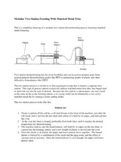
1 Application Report SNOA626B July 1979 Revised May 2013. AN-222 Super Matched Bipolar Transistor Pair sets New Standards for Drift and Noise .. ABSTRACT. This application report discusses how a Super Matched Bipolar Transistor pair sets new standards for drift and noise. Contents 1 Overview .. 2. 2 Approaching Theoretical Noise .. 3. 3 Reactive Sources .. 4. 4 Bandwidth Considerations .. 5. 5 Low Noise Applications .. 6. 6 Low-Noise, Low-Drift Instrumentation Amplifier has Wide Bandwidth .. 9. 7 Low Drift Designs .. 10. 8 Voltage Reference .. 13. 9 Strain Gauge Amplifier .. 14. 10 Thermocouple Amplifier with Cold Junction Compensation .. 15. 11 Power Meter .. 17. 12 Low Cost Mathematical Functions .. 18. Multiplier/Divider .. 18. Square Root .. 20. Squaring Function .. 21. 13 Reference .. 21. List of Figures 1 Noise Figure vs Source Impedance .. 4. 2 High Frequency Power Supply Rejection.
2 5. 3 Ultra Low Noise RIAA Phono Preamplifier .. 7. 4 Ultra Low Noise Preamplifier .. 8. 5 Low Drift-Low Noise Instrumentation Amplifier .. 9. 6 Zeroing Offset and Drift .. 10. 7 Low Frequency Noise of Differential Pair .. 11. 8 Correcting for Residual or Source Generated Drift .. 12. 9 Micropower Reference .. 13. 10 Strain Gauge Instrumentation Amplifier .. 14. 11 Thermocouple Amplifier with Cold-Junction Compensation .. 15. 12 Power Meter (1 kW ) .. 17. 13 High Accuracy One Quadrant Multiplier/Divider .. 19. 14 Low Cost Accurate Squaring Circuit .. 20. 15 Low Cost Accurate Squaring Circuit IOUT = 10 6 (VIN)2 .. 21. All trademarks are the property of their respective owners. SNOA626B July 1979 Revised May 2013 AN-222 Super Matched Bipolar Transistor Pair sets New Standards for Drift 1. Submit Documentation Feedback and Noise Copyright 1979 2013, Texas Instruments Incorporated Overview 1 Overview Matched Bipolar Transistor pairs are a very powerful design tool, yet have received less and less attention over the last few years.
3 This is primarily due to the proliferation of high-performance monolithic circuits that are replacing many designs previously implemented with discrete components. State-of-the-art circuitry, however, is still the realm of the discrete component, especially because of recent improvements in the components themselves. It has become clear in the past few years that ultimate performance in monolithic Transistor pairs was being limited by statistical fluctuations in the material itself and in the processing environment. This led to a Matched Transistor pair fabricated from many different individual transistors physically located in a manner which tended to average out any residual process or material gradients. At the same time, the large number of parallel devices would reduce random fluctuations by the square root of the number of devices. The LM194 is the end result.
4 It is a monolithic Bipolar Matched Transistor pair that offers an order-of- magnitude improvement in matching properties and parasitic base and emitter resistance over conventional Transistor pairs. This was accomplished without compromising breakdown voltage or current gain. The LM194 is specified at 40V minimum collector-to-emitter breakdown voltage and has a minimum hFE of 500 at 1 mA collector current. Maximum offset voltage is 50 V over a collector current range of 1. A to 1 mA. Maximum hFE mismatch is 2%. Common mode rejection of offset voltage (dVOS/dVCB) is 124. dB minimum. An added benefit of paralleling many transistors is the resultant drop in overall rbb and ree, which are 40 and respectively. This makes the logarithmic conformity of emitter-base voltage to collector current excellent even at higher current levels where other devices become non-theoretical.
5 In addition, broadband noise is extremely low, especially at higher operating currents. The key to the success of the LM194 is the nearly one-to-one correlation between measured parameters and those predicted by a theoretical Bipolar Transistor model. The relationship between emitter-base voltage and collector current, for instance, is perfectly logarithmic over an extremely wide range of collector currents, deviating in the pA range because of leakage currents and above several milliamperes due to the finite emitter resistance. This gives the LM194 a distinct advantage in non-linear designs where true logarithmic behavior is essential to circuit accuracy. Of equal importance is the absolute nature of the logarithmic constant, both between the two halves of the device and from unit to unit. The relationship can be expressed as: (1). This relationship holds true both within a single Transistor where IC1 and IC2 represent two different operating currents and between the two halves of the LM194 where collector currents are unbalanced.
6 Of particular importance is the fact that the kT/q logarithmic constant is an absolute quantity dependent only on Boltzman's constant (k), absolute temperature (T), and the charge on the electron (q). Since these values are independent of processing, there is virtually no variation from unit to unit at a fixed temperature. Lab measurements indicate that the logarithmic constant measured at a 10:1 collector current ratio does not vary more than from its theoretical value. Applications such as logarithmic converters, multipliers, thermometers, voltage references, and voltage-controlled amplifiers can take advantage of this inherent accuracy to provide adjustment-free precision circuits. 2 AN-222 Super Matched Bipolar Transistor Pair sets New Standards for Drift SNOA626B July 1979 Revised May 2013. and Noise Submit Documentation Feedback Copyright 1979 2013, Texas Instruments Incorporated Approaching Theoretical Noise 2 Approaching Theoretical Noise In many low-level amplifier applications, the limiting factor on performance is noise.
7 With Bipolar transistors, the theoretical value for emitter-base voltage noise is a function only of absolute temperature and collector current. (2). This formula indicates that voltage noise can be reduced to low levels by simply raising collector current. In fact, that is exactly what happens until collector current reaches a level where parasitic Transistor noise limits any further reduction. This noise floor is usually created by and modeled as an equivalent resistor (rbb ) in series with the base of the Transistor . Low parasitic base resistance is therefore an important factor in ultra-low-noise applications where collector current is pushed to the limits. The 40 equivalent rbb of the LM194 is considerably lower than that of other small-signal transistors. In addition, this device has no excess noise at lower current levels and coincides almost exactly with the predicted values.
8 A low-noise design can be done on paper with a minimum of bench testing. Another noise component in Bipolar transistors is base current noise. For any finite source impedance, current noise must be considered as a quadrature addition to voltage noise. (3). where rs is the source impedance (4). In the LM194, base current noise is a well-defined function of collector current and can be expressed as: (5). To find the collector current which yields the minimum overall equivalent input noise with a given source impedance, the total noise formula can be differentiated with respect to IC and set equal to zero for finding a minimum. (6). (7). For very low source impedances, the 40 rbb of the LM194 should be added to rs in this calculation. A plot of noise figure versus collector current (see curve) shows that the formula does indeed predict the optimum value. The curves are very shallow, however, and actual current can be varied by 3:1 without losing more than 1 dB noise figure in most cases.
9 This may be a worthwhile tradeoff if low bias current (IC. < Iopt) or wide bandwidth (IC > Iopt) is also important. Figure 1 is a plot of best obtainable noise figure versus source impedance for the LM194 and a very low noise junction FET (PF5102). Collector current for the LM194 is optimized for each source impedance and is also plotted on the graph using the right side scale. The PF5102 is operated at a constant 1 mA. It is obvious that the Bipolar device gives significantly better noise figures for low source impedances and/or low frequencies. FETs are particularly poor at very low frequencies (< 10 Hz) and offer advantages only for very high source impedances. SNOA626B July 1979 Revised May 2013 AN-222 Super Matched Bipolar Transistor Pair sets New Standards for Drift 3. Submit Documentation Feedback and Noise Copyright 1979 2013, Texas Instruments Incorporated Reactive Sources Figure 1.
10 Noise Figure vs Source Impedance 3 Reactive Sources Calculations may also be done to derive an optimum collector current when the signal source is reactive. In this case, upper and lower frequencies (fH and fL) must be specified. Also, optimum current is different for an amplifier with a summing junction input (ZIN = 0) as compared to a high impedance input (ZIN XC, XL). The formulas below give optimum collector current for noise within the frequency band fL to fH. For audio applications, lowest perceived noise may be somewhat different because of the variation in sensitivity of the ear to frequencies in the audio range (Fletcher-Munson effect). Capacitive source into high impedance: (8). Capacitive source into summing junction: (9). Inductive source into high impedance: (10). Keep in mind that the simple formula for total input-referred noise, though accurate in itself, does not take into account the effects of noise created in additional stages or noise injected from supply lines.