Transcription of Bidirectional Matched Amplifier - W7ZOI
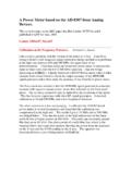
1 A Termination Insensitive Amplifier for Bidirectional Transceivers Wes Hayward, W7ZOI , and Bob Kopski, k3nhi. 26 June 09. The BITX-20 was the first of a now popular class of single-band homebrew SSB. transceivers originally described by Ashhar Farhan, VU3 ICQ. While the original design operated in the 20 meter band, variations have now been built for almost all of the HF. spectrum. The architecture chosen by Farhan was aimed at efficient utilization of critical components. Specifically, the transmit and receive functions share a crystal filter, transmit mixer, LC bandpass filter, and product detector/balanced modulator. These components can do double duty because the Amplifier circuits are Bidirectional . That is, a control voltage applied to an Amplifier determines the direction of signal flow. One of the Bidirectional amplifiers from Farhan's original transceiver is shown in Fig 1. To 220 To Mixer 1K Crystal 220 10 Filter 100. +12R. 220. 1K. 220. 10. 100. +12T. Fig 1. Bidirectional feedback Amplifier used in the BITX-20.
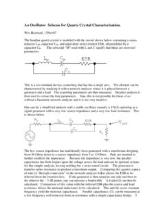
2 With +12R applied, the signal flow is left to right; direction is reversed with +12T. Only one Amplifier operates at one time. These transistors are biased for a current of 8 mA. Amplifier characteristic resistance is 170 Ohms. The characteristic resistance of an Amplifier is the natural impedance for the circuit. When this impedance is presented at one port (output or input), the same resistance is seen at the other port. When an Amplifier is terminated in something other than the characteristic Amplifier resistance, a much different impedance appears at the other port. This behavior is presented in Fig 2. Fig 2. Input Z versus load resistance for the 170 Ohm Amplifier of Fig 1. This is a calculated result with a simple model, but measurement results are similar. 170 Ohms might be a reasonable termination for a crystal filter at 10 or 11 MHz, the usual BITX IF. However, it is a poor termination for the mixer. Of even greater importance, the impedance looking into the crystal filter varies dramatically with frequency.
3 These ill defined impedances are presented to the feedback Amplifier output to create other related frequency dependent terminations for the crystal filter. The ideal Amplifier is one that has an input impedance that does not depend upon the output load. Further, the output impedance should not depend upon the source at the Amplifier input. Such circuits are described as termination insensitive and are easily realized when negative feedback is not used. Negative feedback is still desired, for it establishes gain and impedance while eliminating strong dependence on transistor type and biasing. Our design for this application is shown in Fig 3. 10. R1 +12V_Right Rf 330 50 Ohms 10K 680 Q2. Q3. Q1 2N3904. In/Out 2N3904 Out/In 2N3904 mA 47 mA mA R2. rd 470. 180 15. 50 Ohms 10. +12V_Left 47 2N3904. 330. Q5 680 Q6. 10K. Q4. 2N3904 2N3904. 470 15 180. Fig 3. A Bidirectional 50 Ohm Amplifier with a gain of 15 dB in either direction. The Amplifier is well Matched at both ports, independent of the termination at the other port.
4 The circuit of Fig 3 was designed for 50 Ohm port impedances. However, other values could be used with this basic scheme. How it works: The first stage, Q1, with input at the left is the familiar feedback Amplifier . However, it operates with a fixed load, R1, of 330 Ohms. This fixed value is buffered from the output load through Q2/Q3. The value for R1 is reflected through Amplifier Q1. The feedback resistor (Rf=680) and the emitter degeneration (rd=15) in combination with the load, R1, set the input at 50 Ohms. These parts also establish the gain. The design equations are found on the web: An appendix to this report derives the equations. The output circuit is a Darlington emitter follower, Q2 and Q3, which has near unity voltage gain. A 47 Ohm series output resistor, R2, establishes the Amplifier output impedance. The relatively high input impedance of Q2 isolates the internal load R1. from the output. The circuit of Fig 3 was built and tested and is shown in a following photo.
5 The intrinsic termination sensitivity that we see with feedback amplifiers results from the parallel feedback. Emitter degeneration does not produce the sensitivity. Fig 4. Photo of the Amplifier from Fig 3. SMA connectors were used to facilitate measurements while ugly construction allowed a quick build. This Amplifier was carefully evaluated. The gain is 15 dB in both directions. If only one Amplifier is connected, the gain increases to dB. This is the value predicted in Linear Technology SPICE simulations. The measured input return loss was 29 dB at 10 MHz and changed little when the output load was changed from 50 Ohms to an open circuit. The output RL was 26 dB and was again independent of the input termination. Gain was flat within 1 dB from 1 to 50. MHz; RL was better than 20 dB over the same span. The reverse attenuation was 60 dB. when one of the amplifiers was investigated with the other disconnected. The large signal behavior is reasonable, although not in the class desired for a wide dynamic range receiver application.
6 The circuit was tested with a two tone signal from a pair of signal generators with the result that OIP3=+ dBm. This value increased to +22 dBm when the off Amplifier for the other direction was disconnected. SPICE. simulation produced OIP3=+ dBm. Large signal performance could be enhanced with greater bias current in larger transistors. The gain compression performance of this Amplifier was not measured. However, measurement of a similar circuit showed a P(-1 dB) that was below the output intercept by about 17 dB. That would put this circuit at P(-1 dB) + dBm. A rule of thumb suggesting a 16 dB difference has been with us since antiquity. Spot noise figure was measured using a Noise Comm diode in a calibrated noise source. (Sabin, QST, May 1994) The 10 MHz noise figure was dB for the circuit of Fig 3. An earlier Amplifier with 3 mA emitter current in the input transistor and higher gain produced slightly lower noise figure. Extensions and Refinements The first thing that we will want to change is gain.
7 Some calculated suggestions are shown in the following table. Fig 5. Alternative designs that provide a variety of gains. These amplifiers are all designed for 50 Ohm terminations. The gain in one direction need not equal that in the other. It would sometimes be useful to have amplifiers with terminations other than 50 Ohms. There is no strong reason why the ports even need to be the same. The reader can realize these variations with the design procedures in the references. Other amplifiers are also capable of either being termination insensitive, or at least have reduced sensitivity. One example is a cascade of two transformer feedback amplifiers with a pad between them. (EMRFD, Fig ) There are certainly other designs and the solutions presented here are most likely not unique. One simple Amplifier that we have found extremely useful consists of a common base Amplifier followed by a common collector stage with a series output resistance. This is shown below. +12V. 330. Q2.
8 Q1. 10. 10 47 270. 47 120. Fig 6. A simple termination insensitive Amplifier with good bandwidth. This could be adapted to become Bidirectional . We built one of these amplifiers with 2N3904 transistors and measured it at 10 MHz. The results were gain=10 dB, NF= dB, excellent return loss at both ports, OIP3=+ dBm, and Pout(-1 dB)=+9 dBm. Other than a compromised noise figure, this is a hard circuit to beat. The wideband performance is enhanced by changing to hotter transistors (2N5179 or similar) and adding a small inductance in series with the 330 Ohm Q1 collector resistor. In one example, a cascade of three of these stages exhibited a 3 dB BW of over 100 MHz. A new transistor will not substantially improve noise figure, for the high NF is a result of the circuit topology. The reader may have noticed that none of the circuits presented used transformers. That is not necessary. A termination insensitive Amplifier with a transformer output is shown below. Indeed, it was this design that got this project started for the two of us.
9 +12V :1. turns RL1=470 ratio 10K 470. 10K 1K. Q2. Q1. 10 150. 390 200. Fig 7. An Amplifier using an output transformer with reduced termination sensitivity. A transformer output allows higher output intercept and gain compression powers for a given current in Q2. Transformer design is important. Gain may be slightly altered by changing degeneration in Q2. This circuit was measured over a wide frequency range with results included in the referenced report. Transformers measurement was useful. Conclusions We believe the relatively simple amplifiers presented will be useful for the folks building BITX transceivers or similar Bidirectional designs. The ultimate proof is, of course, a complete transceiver design using these circuits, including measured results. We have emphasized designs that use no transformers, but still offer termination insensitivity. Transformer designs can certainly be useful, but care must be devoted to these components. The designs presented here are intended to drop into a 50 Ohm environment.
10 We still prefer 50 Ohm gain blocks, even when it may not be necessary, for it allows relatively easy module measurements to be performed. Impedance transformations may be built into other blocks such as crystal filters when needed. There are certainly other designs that may be suitable for a termination insensitive Amplifier . The important consideration for a SSB transceiver is not the exact Amplifier topology, but just the realization that careful impedance matching is a vital part of the overall design.