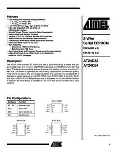
Transcription of Two-wire Serial EEPROM - Microchip Technology
1 1 Features Low-voltage and Standard-voltage Operation (VCC = to ) (VCC = to ) Internally Organized 128 x 8 (1K), 256 x 8 (2K), 512 x 8 (4K),1024 x 8 (8K) or 2048 x 8 (16K) Two-wire Serial Interface Schmitt Trigger, Filtered Inputs for Noise Suppression Bidirectional Data Transfer Protocol 100 kHz ( ) and 400 kHz ( , 5V) Compatibility Write Protect Pin for Hardware Data Protection 8-byte Page (1K, 2K), 16-byte Page (4K, 8K, 16K) Write Modes Partial Page Writes Allowed Self-timed Write Cycle (5 ms max) High-reliability Endurance: 1 Million Write Cycles Data Retention: 100 Years Automotive Devices Available 8-lead JEDEC PDIP, 8-lead JEDEC SOIC, 8-lead Ultra Thin Mini-MAP (MLP 2x3), 5-lead SOT23, 8-lead TSSOP and 8-ball dBGA2 Packages Die Sales: Wafer Form, Waffle Pack and Bumped WafersDescriptionThe AT24C01A/02/04/08A/16A provides 1024/2048/4096/8192/16384 bits of serialelectrically erasable and programmable read-only memory ( EEPROM ) organized as128/256/512/1024/2048 words of 8 bits each.
2 The device is optimized for use in manyindustrial and commercial applications where low-power and low-voltage operationare essential. The AT24C01A/02/04/08A/16A is available in space-saving 8-leadPDIP, 8-lead JEDEC SOIC, 8-lead Ultra Thin Mini-MAP (MLP 2x3), 5-lead SOT23(AT24C01A/AT24C02/AT24C04), 8-lead TSSOP, and 8-ball dBGA2 packages and isaccessed via a Two-wire Serial interface. In addition, the entire family is available ( to ) and ( to ) versions. Table 1. Pin ConfigurationPin NameFunctionA0 - A2 Address InputsSDAS erial DataSCLS erial Clock Input WPWrite ProtectNCNo ConnectGNDG roundVCCP ower SupplyTwo-wireSerial EEPROM1K (128 x 8)2K (256 x 8)4K (512 x 8)8K (1024 x 8)16K (2048 x 8)AT24C01A(1)AT24C02(2)AT24C04AT24C08 AAT24C16A(3)0180Z1 SEEPR 5/07 Notes:1.
3 Not Recommended fornew design; Pleaserefer to Not Recommended fornew design; Pleaserefer to Not Recommended fornew design; Pleaserefer to AT24C16 Bdatasheet8-lead SOIC12348765A0A1A2 GNDVCCWPSCLSDA8-lead PDIP12348765A0A1A2 GNDVCCWPSCLSDA8-lead Ultra Thin Mini-MAP (MLP 2x3)Bottom View12348765 VCCWPSCLSDAA0A1A2 GND5-lead SOT2312354 SCLGNDSDAWPVCC8-ball dBGA2 Bottom ViewVCCWPSCLSDAA0A1A2 GND123487658-lead TSSOP12348765A0A1A2 GNDVCCWPSCLSDA2AT24C01A/02/04/08A/16A018 0Z1 SEEPR 5/07 Figure 1. Block DiagramAbsolute Maximum RatingsOperating 55 C to +125 C*NOTICE:Stresses beyond those listed under Absolute Maximum Ratings may cause permanent dam-age to the device.
4 This is a stress rating only and functional operation of the device at these or any other conditions beyond those indicated in the operational sections of this specification is not implied. Exposure to absolute maximum rating conditions for extended periods may affect device Temperature .. 65 C to +150 CVoltage on Any Pinwith Respect to Ground .. to + Operating Voltage .. Output mA3AT24C01A/02/04/08A/16A0180Z1 SEEPR 5/07 Pin DescriptionSERIAL CLOCK (SCL): The SCL input is used to positive edge clock data into eachEEPROM device and negative edge clock data out of each DATA (SDA): The SDA pin is bidirectional for Serial data transfer.
5 This pin isopen-drain driven and may be wire-ORed with any number of other open-drain or open-collector ADDRESSES (A2, A1, A0): The A2, A1 and A0 pins are deviceaddress inputs that are hard wired for the AT24C01A and the AT24C02. As many aseight 1K/2K devices may be addressed on a single bus system (device addressing isdiscussed in detail under the Device Addressing section).The AT24C04 uses the A2 and A1 inputs for hard wire addressing and a total of four 4 Kdevices may be addressed on a single bus system. The A0 pin is a no connect and canbe connected to AT24C08A only uses the A2 input for hardwire addressing and a total of two 8 Kdevices may be addressed on a single bus system.
6 The A0 and A1 pins are no connectsand can be connected to AT24C16A does not use the device address pins, which limits the number ofdevices on a single bus to one. The A0, A1 and A2 pins are no connects and can beconnected to PROTECT (WP): The AT24C01A/02/04/08A/16A has a Write Protect pin thatprovides hardware data protection. The Write Protect pin allows normal Read/Writeoperations when connected to ground (GND). When the Write Protect pin is connectedto VCC, the write protection feature is enabled and operates as shown in Table 2. Write ProtectMemory OrganizationAT24C01A, 1K Serial EEPROM : Internally organized with 16 pages of 8 bytes each,the 1K requires a 7-bit data word address for random word addressing.
7 AT24C02, 2K Serial EEPROM : Internally organized with 32 pages of 8 bytes each,the 2K requires an 8-bit data word address for random word addressing. AT24C04, 4K Serial EEPROM : Internally organized with 32 pages of 16 bytes each,the 4K requires a 9-bit data word address for random word addressing. AT24C08A, 8K Serial EEPROM : Internally organized with 64 pages of 16 byteseach, the 8K requires a 10-bit data word address for random word addressing. AT24C16A, 16K Serial EEPROM : Internally organized with 128 pages of 16 byteseach, the 16K requires an 11-bit data word address for random word addressing. WP PinStatusPart of the Array Protected24C01A24C0224C0424C08A24C16 AAt VCCFull (1K) ArrayFull (2K) ArrayFull (4K) ArrayFull (8K) ArrayFull (16K) ArrayAt GNDN ormal Read/Write Operations4AT24C01A/02/04/08A/16A0180Z1 SEEPR 5/07 Note:1.
8 This parameter is characterized and is not 100% :1. VIL min and VIH max are reference only and are not tested. Table 3. Pin Capacitance(1)Applicable over recommended operating range from TA = 25 C, f = MHz, VCC = + ConditionMaxUnitsConditionsCI/OInput/Out put Capacitance (SDA)8pFVI/O = 0 VCINI nput Capacitance (A0, A1, A2, SCL)6pFVIN = 0 VTable 4. DC CharacteristicsApplicable over recommended operating range from: TAI = 40 C to +85 C, VCC = + to + , VCC= + to + (unless otherwise noted)SymbolParameterTest ConditionMinTypMaxUnitsVCC1 Supply Current VCC = at 100 Current VCC = at 100 Current VCC = = VCC or AISB2 Standby Current VCC = = VCC or AISB3 Standby Current VCC = = VCC or AISB4 Standby Current VCC = = VCC or AILII nput Leakage CurrentVIN = VCC or AILOO utput Leakage CurrentVOUT = VCC or AVILI nput Low Level(1) x High Level(1)VCC x + Low Level VCC = = Low Level VCC = = SEEPR 5/07 Note:1.
9 This parameter is 5. AC CharacteristicsApplicable over recommended operating range from TAI = 40 C to +85 C, VCC = + to + , VCC = + to + ,CL = 1 TTL Gate and 100 pF (unless otherwise noted) , Frequency, SCL100400kHztLOWC lock Pulse Width stHIGHC lock Pulse Width stINoise Suppression Time(1)10050nstAAClock Low to Data Out stBUFTime the bus must be free before a new transmission can start(1) Hold Setup In Hold Time00 In Setup Time200100nstRInputs Rise Time(1) stFInputs Fall Time(1) Setup stDHData Out Hold Time10050nstWRWrite Cycle Time55msEndurance(1) , 25 C, Byte Mode1M1 MWrite Cycles6AT24C01A/02/04/08A/16A0180Z1 SEEPR 5/07 Device Operation CLOCK and DATA TRANSITIONS: The SDA pin is normally pulled high with an exter-nal device.
10 Data on the SDA pin may change only during SCL low time periods (seeFigure 4 on page 7). Data changes during SCL high periods will indicate a start or stopcondition as defined CONDITION: A high-to-low transition of SDA with SCL high is a start conditionwhich must precede any other command (see Figure 5 on page 8).STOP CONDITION: A low-to-high transition of SDA with SCL high is a stop a read sequence, the stop command will place the EEPROM in a standby powermode (see Figure 5 on page 8).ACKNOWLEDGE: All addresses and data words are serially transmitted to and fromthe EEPROM in 8-bit words. The EEPROM sends a zero to acknowledge that it hasreceived each word.