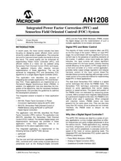
Transcription of UCC28070 Interleaving Continuous Conduction Mode PFC ...
1 + VINVOUT12V to 21VM2 RBRARBM1L2D2D1 COUTRACPCCPCCZCCZCRZCRZCCSSRRDMRRTT1T2 CCDRRDMXRSYNCREFRPK1 RPK2 CZVRZVCPVRSRS123456789102019181716151413 1211 CAOACAOBPKLMTGNDVAOVINACVSENSECSACSBRTCD RSSGDBGDAIMOVCCRSYNTHVREFDMAXRDMRIMOTo CSBTo CSAFrom IxfrmsL1 Copyright 2016, Texas Instruments IncorporatedProductFolderSample &BuyTechnicalDocumentsTools &SoftwareSupport &CommunityReferenceDesignAn IMPORTANTNOTICEat the end of this datasheetaddressesavailability,warranty, changes,use in safety-criticalapplications,intellectual propertymattersand NOVEMBER2007 REVISEDAPRIL2016 UCC28070 InterleavingContinuousConductionMode PFC Controller11 Features1 InterleavedAverageCurrent-ModePWMC ontrolWithInherentCurrentMatching AdvancedCurrentSynthesizerCurrentSensing for SuperiorEfficiency Highly-LinearMultiplierOutputWithInterna lQuantizedVoltageFeed-ForwardCorrectionf orNear-UnityPF ProgrammableFrequencyfrom30 kHz to 300 kHz ProgrammableMaximumDuty-CycleClamp ProgrammableFrequency-DitheringRateandMa gnitudefor EnhancedEMI Reduction Magnitude:3 kHz to 30 kHz Rate.
2 Up to 30 kHz External-ClockSynchronizationCapability EnhancedLoadand Line TransientResponsethroughVoltageAmplifier OutputSlew-RateCorrection ProgrammablePeakCurrentLimiting Bias-SupplyUVLO,OvervoltageProtection,Op en-LoopDetection,and PFC-EnableMonitoring ExternalPFC-DisableInterface Open-CircuitProtectionon VSENSEand VINAC pins ProgrammableSoft-Start2 Applications High-EfficiencyServerand DesktopPowerSupplies TelecomRectifiers WhiteGoodsand IndustrialEquipment3 DescriptionTheUCC28070is an advancedpowerfactorcorrection(PFC)device thatintegratestwo pulse-widthmodulators(PWMs)operating180 out the inputand outputripplecurrents, significantlyimprovedmultiplierdesignpro videsa sharedcurrentreferenceto two independentcurrentamplifiersthatensuresm atchedaverage-currentmodecontrolinbothPW Moutputswhilemaintaininga stable,low-distortion, UCC28070devicecontainsmultipleinnovation sincludingcurrentsynthesisandquantizedvo ltagefeed-forwardto promoteperformanceenhancementsin PF,efficiency,THD, ,clocksynchronization,and slewrate enhancementfurtherexpandthe varietyofprotectionfeaturesincludingoutp ut-overvoltagedetection,programmablepeak -currentlimit,undervoltagelockout,and (1)PARTNUMBERPACKAGEBODYSIZE(NOM)UCC2807 0 DWSOIC(20) (20) (20) (20) (20) (20) (1)
3 For all availablepackages,see the orderableaddendumatthe end of the NOVEMBER2007 : UCC28070 SubmitDocumentationFeedbackCopyright 2007 2016,TexasInstrumentsIncorporatedTableof Contents1 Pin Configurationand Applicationand Deviceand Mechanical,Packaging,and RevisionHistoryNOTE:Pagenumbersfor previousrevisionsmay differfrompagenumbersin the (April2011)to RevisionFPage AddedESDR atingstable,FeatureDescriptionsection,De viceFunctionalModes,Applicationand Implementationsection,PowerSupplyRecomme ndationssection,Layoutsection,Deviceand DocumentationSupportsection,andMechanica l,Packaging,and (June2010)to RevisionEPage (June2009)to RevisionDPage Changed30 kHz to 300 kHz ..11 CDR20 DMAX2 RDM19 RT3 VAO18 SS4 VSENSE17 GDB5 VINAC16 GND6 IMO15 VCC7 RSYNTH14 GDA8 CSB13 VREF9 CSA12 CAOA10 PKLMT11 NOVEMBER2007 REVISEDAPRIL2016 ProductFolderLinks.
4 UCC28070 SubmitDocumentationFeedbackCopyright 2007 2016,TexasInstrumentsIncorporated5 Pin Configurationand FunctionsDW and PW Packages20-PinSOICand TSSOPTop ViewPin phaseA the invertinginputof phaseA PWMcomparatorfor currentregulationloop compensationcomponentsbetweenthis pin and phaseB the invertinginputof phaseB PWMcomparatorfor currentregulationloop compensationcomponentsbetweenthis pin and An externalcapacitorto GNDprogramsthe rate CDRpin to the VREFpin to ON-timeof GDA,CSAis internallyconnectedto the invertinginputofphaseA currentamplifierthroughthe ON-timeof GDB,CSBis internallyconnectedto the invertinginputofphaseB currentamplifierthroughthe A resistorto GNDsets the PWMmaximumduty-cyclebasedon the ratioof RDMX/ limited-currentoutputis intendedto connectto a separategate-drivedevicesuitablefor drivingthe phaseA switchingcomponent(s).
5 The outputvoltageis typicallyclampedto limited-currentoutputis intendedto connectto a separategate-drivedevicesuitablefor drivingthe phaseB switchingcomponent(s).The outputvoltageis typicallyclampedto compensationand programmingresistorand capacitornetworksto thispin. Connectthis pin to the systemthrougha separatetracefor resistorbetweenthis pin and GNDto set the resistor-dividernetworkbetweenVREFand this pin to set thevoltagethresholdof the desired (SYNC) externalsynchronizationpin. An externalresistorto GNDprogramsthe magnitudeof disabled(CDR> 5 V), the internalmasterclocksynchronizesto positiveedgespresentedon the RDMpin. ConnectRDMto GNDwhenditheringis disabledand synchronizationis not NOVEMBER2007 : UCC28070 SubmitDocumentationFeedbackCopyright 2007 2016,TexasInstrumentsIncorporatedPin Functions(continued) resistorbetweenthis pin and GNDto set themagnitudeof the VREF disablescurrentsynthesisandconnectCSAand CSBdirectlyto A resistorto GNDsets the runningfrequencyof capacitorto GNDon this pin to set the soft-startslewratebasedon an internally-fixed,10- A regulationreferencevoltagefor VSENSEis clampedtoVSSuntil VSSexceeds3 V.
6 Uponrecoveryfromcertainfault conditions,a 1-mAcurrentsourceis presentat theSS pin until the SS voltageequalsthe SS pin V immediatelydisablesbothGDAand themultiplierinputand the voltageregulationloop compensationcomponentsbetweenthis pin and F ceramicbypasscapacitoras closeas possibleto this pin and Line the multiplierand negativeterminalof the resistor-dividernetworkbetweenVIN, VINAC,and GNDidenticaltothe PFCoutputdividernetworkconnectedat ReferenceVoltageand F ceramicbypasscapacitoras closeaspossibleto this pin and the invertinginputof the transconductancevoltageerroramplifierin additionto the positiveterminalof the theOVP,PFCenable,and PFCoutputwith a resistor-dividernetwork.(1)Stressesbeyon dthoselistedunderAbsoluteMaximumRatingsm ay causepermanentdamageto the stressratingsonly,whichdo not implyfunctionaloperationof the deviceat theseor any otherconditionsbeyondthoseindicatedunder RecommendedOperatingConditions.
7 Exposureto absolute-maximum-ratedconditionsfor extendedperiodsmay (unlessotherwisenoted)(1)MINMAXUNITS upplyvoltageVCC22 VSupplycurrent,IVCC20mAGatedrivecurrent continuousGDA,GDB pulsedGDA,GDB ,GDB + ,RDM,RT, CDR,VINAC,VSENSE,SS, VAO,IMO,CSA,CSB,CAOA,CAOB,PKLMT,VREF , DMAX,RDM,RSYNTH ,VAO,CAOA,CAOB,IMO10 Leadtemperature(10 seconds)260 COperatingjunctiontemperature,TJ 40125 CStoragetemperature,Tstg 65150 C(1)JEDEC documentJEP155statesthat 500-VHBM allowssafe manufacturingwith a standardESDcontrolprocess.(2)JEDEC documentJEP157statesthat 250-VCDM allowssafe manufacturingwith a (ESD)ElectrostaticdischargeHuman-bodymod el(HBM),per ANSI/ESDA/JEDECJS-001(1)2000 VCharged-devicemodel(CDM),per JEDEC specificationJESD22-C101(2) NOVEMBER2007 REVISEDAPRIL2016 ProductFolderLinks.
8 UCC28070 SubmitDocumentationFeedbackCopyright 2007 2016, (unlessotherwisenoted)MINMAXUNITVCCI nputvoltage(froma low-impedancesource)VCCVUVLO+ 1 , RRDMRDM resistance30330k (1)For moreinformationabouttraditionaland new thermalmetrics,see theSemiconductorand IC PackageThermalMetricsapplicationreport, (1) UCC28070 UNITSOIC(DW)TSSOP(PW)20 PINS20 PINSR C/WR JC(top)Junction-to-case(top) C/WR C/W C/W C/W(1)ExcessiveVCCinputvoltageor currentdamagesthe clampdoesnot protectthe devicefroman anunregulatedsupplyis used,TI recommendsa series-connectedfixedpositivevoltageregu latorsuchas a UA78L15A. SeeAbsoluteMaximumRatingsfor the limitson VCCvoltageand 40 C to 125 C, TJ= TA, VCC= 12 V, GND= 0 V, RRT= 75 k , RDMX= , RRDM= RSYN= 100 k , CCDR= nF,CSS= CVREF= F, CVCC= 1 F, IVREF= 0 mA (unlessotherwisenoted)PARAMETERTESTCONDI TIONSMINTYPMAXUNITBIASSUPPLYVCC(SHUNT)VC Cshuntvoltage(1)IVCC= 10 mA232527 VIVCCS upplycurrentdisabledVVSENSE= 0 V7mAenabledVVSENSE= 3 V (switching)912 UVLOVCC= 7 V200 AVCC= 9 V46mAVUVLOUVLO turnonthresholdMeasuredat VCC(rising) VCC(falling)1 VREF enablethresholdMeasuredat VCC(rising) loadIVREF= 0 the changein VVREF(IVREF= 0 mA and 2 mA) 1212mVlinerejectionMeasuredas the changein VVREF(VCC= 11 V and 20 V, IVREF= 0 A) 12126 UCC28070 SLUS794F NOVEMBER2007.
9 UCC28070 SubmitDocumentationFeedbackCopyright 2007 2016,TexasInstrumentsIncorporatedElectri calCharacteristics(continued)TA= 40 C to 125 C, TJ= TA, VCC= 12 V, GND= 0 V, RRT= 75 k , RDMX= , RRDM= RSYN= 100 k , CCDR= nF,CSS= CVREF= F, CVCC= 1 F, IVREF= 0 mA (unlessotherwisenoted)PARAMETERTESTCONDI TIONSMINTYPMAXUNIT(2)Due to the influenceof the synchronizationpulsewidthon the programmabilityof the maximumPWMswitchingduty cycle(DMAX), TIrecommendsminimizingthe synchronizationsignalduty VSENSE(rising) SS (falling) > GDB179180181 VDMAX,VRT, andVRDMT imingregulationvoltagesMeasuredat DMAX,RT, and 75 k , RDMX= ,VRDM= 0 V, VCDR= 6 V95100105kHzRRT= , RDMX= ,VRDM= 0 V, VCDR= 6 V270290330 DMAXDuty-cycleclampRRT= 75 k , RDMX= ,VRDM= 0 V, VCDR= 6 V92%95%98%MinimumprogrammableOFF-timeRRT = , RDMX= ,VRDM= 0 V, VCDR= 6 V50150250nsfDMFrequencyditheringmagnitud echangein fPWMRRDM= 316 k , RRT= 75 k 234kHzRRDM= , RRT= 243036fDRFrequencyditheringrate of changein fPWMCCDR= nF, RRDM= 100 k 3kHzCCDR= nF, RRDM= 100 k 20 ICDRD itherrate currentMeasuredat CDR(sinkand source) 10 ADitherdisablethresholdMeasuredat CDR(rising) CDR(rising) 6 V, measuredfromRDM(rising)toGDx(rising)5010 0nsSYNC threshold(rising)VCDR= 6 V, measuredat (falling)
10 VCDR= 6 V, measuredat sMaximumduty cycle(2)50%VOLTAGEAMPLIFIERVSENSE voltageIn regulation,TA= 25 currentIn regulation250500nAVAO high voltageVVSENSE= voltageVVSENSE= V to V, VVAO= 3 V70 SVAO sink current,overdrivenlimitVVSENSE= V, VVAO= 3 V30 AVAO sourcecurrent,overdrivenVVSENSE= V, VVAO= 3 V, SS = 3 V 30 AVAO sourcecurrent,overdrivenlimit + ISRCVVSENSE= V, VVAO= 3 V 130 ASlew-ratecorrectionthresholdMeasuredas VVSENSE(falling)/ VVSENSE(regulation)92%93%95% NOVEMBER2007 REVISEDAPRIL2016 ProductFolderLinks: UCC28070 SubmitDocumentationFeedbackCopyright 2007 2016,TexasInstrumentsIncorporatedElectri calCharacteristics(continued)TA= 40 C to 125 C, TJ= TA, VCC= 12 V, GND= 0 V, RRT= 75 k , RDMX= , RRDM= RSYN= 100 k , CCDR= nF,CSS= CVREF= F, CVCC= 1 F, IVREF= 0 mA (unlessotherwisenoted)PARAMETERTESTCONDI TIONSMINTYPMAXUNIT(3)The Level1 thresholdrepresentsthezero-crossingdetec tionthresholdabovewhichVVINAC mustrise to initiatea new inputhalf-cycle,and belowwhichVVINAC mustfall to terminatethat VSENSE(rising)39mVISRCSlew-ratecorrectio ncurrentMeasuredat VAO,in additionto VAOsourcecurrent 100 ASlew-ratecorrectionenablethresholdMeasu redat SS (rising)