Transcription of UNISONIC TECHNOLOGIES CO., LTD
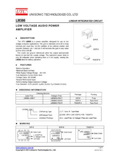
1 UNISONIC TECHNOLOGIES CO., LTD 6N10 Power MOSFET 1 of 5 Copyright 2016 UNISONIC TECHNOLOGIES Co., Ltd Amps, 100 Volts N-CHANNEL POWER MOSFET DESCRIPTION The UTC 6N10 is an N-Channel enhancement mode power FET providing customers with excellent switching performanceand minimum on-state resistance. The UTC 6N10 is generally applied in voltage applications, such as DC motor control, audio amplifier and high efficiency switching DC/DC converters.
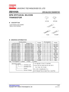
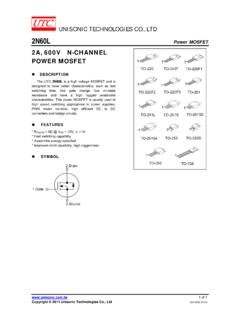
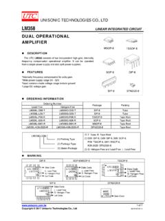
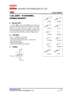
2 FEATURES * RDS(ON) < @ VGS=10V, ID= * Fast switching * Improved dv/dt capability SYMBOL TO-2521TO-252D1 SOT-2231 SOP-8 ORDERING INFORMATION Ordering Number Pin Assignment Lead Free Halogen Free Package 123456 7 8 Packing - 6N10G-AA3-R SOT-223 GDS--- - - Tape Reel6N10L-TN3-R 6N10G-TN3-R TO-252 GDS--- - - Tape Reel6N10L-TND-R 6N10G-TND-R TO-252D GDS--- - - Tape Reel- 6N10G-S08-R SOP-8 SSSGDD D D Tape ReelNote: Pin Assignment: G: Gate D: Drain S: Source 6N10 Power MOSFET UNISONIC TECHNOLOGIES CO.
3 , LTD 2 of 5 MARKING PACKAGE MARKING SOT-223 TO-252 TO-252D SOP-8 UTC6N10G23415678 Date CodeLot Code 6N10 Power MOSFET UNISONIC TECHNOLOGIES CO., LTD 3 of 5 ABSOLUTE MAXIMUM RATINGS (TC =25 C, unless otherwise specified)
4 PARAMETER SYMBOL RATINGS UNIT Drain-Source Voltage VDS 100 V Gate-Source Voltage VGS 20 V Continuous ID A Continuous Drain Current Pulsed IDM A Repetitive Avalanche Energy (Duty Cycle 1%) L= EAR mJ SOT-223 TO-252/TO-252D16 Power Dissipation SOP-8 PD W Junction Temperature TJ +150 C Storage Temperature TSTG -55 ~ +150 C Note.
5 Absolute maximum ratings are those values beyond which the device could be permanently damaged. Absolute maximum ratings are stress ratings only and functional device operation is not implied. THERMAL CHARACTERISTICS PARAMETER SYMBOL RATINGS UNIT SOT-223 150 TO-252/TO-252D110 Junction to Ambient SOP-8 JA 50 C/W SOT-223 TO-252 Junction to Case SOP-8 JC 78 C/W Note.
6 JA is the sum of the junction-to-case and case-to-ambient thermal resistance where the case thermal reference is defined as the solder mounting surface of the drain pins. JC is guaranteed by design while JA is determined by the user s board deign. 6N10 Power MOSFET UNISONIC TECHNOLOGIES CO., LTD 4 of 5 ELECTRICAL CHARACTERISTICS (TJ=25 C, unless otherwise noted)
7 PARAMETER SYMBOLTEST CONDITIONS MIN TYP MAX UNITOFF CHARACTERISTICS Drain-Source Breakdown Voltage BVDSS ID=250 A, VGS=0V 100 V VDS=100V, VGS=0V 1 AVDS=100V, VGS=0V, TJ=125 C 50 ADrain-Source Leakage Current IDSS VDS=100V, VGS=0V, TJ=150 C 250 AForward VGS=+20V, VDS=0V +100nAGate- Source Leakage Current Reverse IGSS VGS=-20V, VDS=0V -100nAOn-State Drain Current (Note 2) ID(on) VDS=5V, VGS=10V A ON CHARACTERISTICS Gate Threshold Voltage VGS(TH)
8 VDS=VGS, ID=250 A VGS=10V, ID=3A , ID=3A, TJ=125 C , ID=3A, TJ=150 C Drain-Source On-State Resistance (Note 2) RDS(ON) VGS= , ID= Forward Transconductance (Note 2) gFS VDS=15V, ID=3A S DYNAMIC PARAMETERS (Note1)
9 Input Capacitance CISS 320 pFOutput Capacitance COSS 80 pFReverse Transfer Capacitance CRSS VGS=0V, VDS=25V, f= 17 pFSWITCHING PARAMETERS Total Gate Charge (Note 3) QG 27 75 nCGate to Source Charge (Note 3) QGS nCGate to Drain Charge (Note 3)
10 QGD VDS=50V, VGS=10V, ID= IG=100 A nCTurn-ON Delay Time (Note3) tD(ON) 28 58 nsRise Time (Note 3) tR 30 60 nsTurn-OFF Delay Time (Note 3) tD(OFF) 148 178nsFall-Time (Note 3) tF VDD=30V, RL= , ID= , VGEN=10V, RG=25 52 82 nsSOURCE- DRAIN DIODE RATINGS AND CHARACTERISTICS (TC=25 C) Maximum Pulsed Drain-Source Diode Forward Current ISM Drain-Source Diode Forward Voltage (Note 2)