Transcription of UNISONIC TECHNOLOGIES CO., LTD
1 UNISONIC TECHNOLOGIES CO., LTD UR6225 CMOS IC 1 of 15 Copyright 2018 UNISONIC TECHNOLOGIES Co., Ltd POSITIVE VOLTAGE REGULATOR DESCRIPTION The UTC UR6225 is a positive voltage output, three-pin regulator that provides a high current even when the input/output voltage differential is small. Low power consumption and high accuracy is achieved through CMOS and laser trimming TECHNOLOGIES . The UTC UR6225 consists of a high-precision voltage reference, an error amplification circuit, and a current limited output driver.
2 Transient responses to load variations have improved in comparison to the existing series. FEATURES * Maximum Output Current: 300mA (Within Max. Power Dissipation, VOUT = ) * Output Voltage Range: ~ in Increments ( ~ for Custom Products) * Highly Accurate: Output Voltage 2%( 1% for Semi-Custom Products) * Low Power Consumption: Typ. A @ VOUT= * Output Voltage Temperature Characteristics: Typ. 100ppm/ С * Input Stability : Typ. * Small Input-Output Differential: IOUT = 100mA @ VOUT = with a Differential.
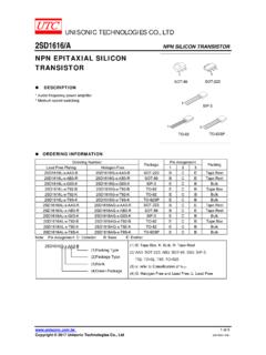
3 ORDERING INFORMATION Ordering Number Pin Assignment Lead Free Halogen Free Package 1234 5 Packing UR6225L-xx-AB3-C-R UR6225G-xx-AB3-C-RSOT-89 GI O- - Tape Reel UR6225L-xx-AE3-3-R UR6225G-xx-AE3-3-RSOT-23 GOI - - Tape Reel UR6225L-xx-AF5-C-R UR6225G-xx-AF5-C-RSOT-25 I GNN O Tape Reel UR6225L-xx-AF5-F-R UR6225G-xx-AF5-F-RSOT-25 GI ON N Tape Reel UR6225L-xx-T92-C-B UR6225G-xx-T92-C-B TO-92 GI O- - Tape Box UR6225L-xx-T92-C-K UR6225G-xx-T92-C-K TO-92 GI O- - Bulk UR6225L-xx-T92-B-B UR6225G-xx-T92-B-B TO-92 OGI - - Tape Box UR6225L-xx-T92-B-K UR6225G-xx-T92-B-K TO-92 OGI.
4 - Bulk Note: Pin Assignment: I: VIN O: VOUT G: VSS N: No Connection xx: Output Voltage, refer to Marking Information. UR6225 CMOS IC UNISONIC TECHNOLOGIES CO., LTD 2 of 15 MARKING INFORMATION PACKAGE VOLTAGE CODE MARKING SOT-89 SOT-25 321 F2XX54 Voltage CodePin CodeL: Lead FreeG: Halogen Free SOT-23 F2XX213 Voltage CodeL: Lead FreeG.
5 Halogen Free TO-92 15 18 20 21 25 26 27 28 2 30 31 33 35 36 38 40 45 50 60 BLOCK DIAGRAM VINVOUTC urrent LimitVoltageReference+-VSS UR6225 CMOS IC UNISONIC TECHNOLOGIES CO., LTD 3 of 15 ABSOLUTE MAXIMUM RATINGS (TA=25 С, unless otherwise specified) PARAMETER SYMBOLRATINGS UNIT Input Voltage VIN 10 V Output Current IOUT 300 mA Output Voltage VOUT ~ VIN+ V SC-23/SOT-25
6 250 mW SOT-89 500 mW Power Dissipation TO-92 PD 300 mW Junction Temperature TJ +125 С Operating Temperature TOPR -40 ~ +85 С Storage Temperature TSTG -40~+125 С Note: Absolute maximum ratings are those values beyond which the device could be permanently damaged.
7 Absolute maximum ratings are stress ratings only and functional device operation is not implied. ELECTRICAL CHARACTERISTICS (TA=25 С, unless otherwise specified) (Note1) PARAMETER CIRCUIT SYMBOL TEST CONDITIONS MIN TYP MAXUNITO utput Voltage 1 VOUT(E)(Note2) IOUT=40mA, VIN= Maximum Output Current 1 IOUT(MAX) VIN= , VOUT(E) 250 mAMinimum Load Current IOUT(MIN)
8 VIN=VOUT+1V 50 A Load Stability 1 VOUT VIN= ,1mA IOUT 100mA 40 80 mV1 VDIF1 IOUT=100mA 120 mVInput-Output Voltage Differential (Note3) 1 VDIF2 IOUT=200mA 380 mVSupply Current 2 ISS VIN= A Input Stability 1 VOUT VIN VOUTIOUT=40mA VIN 10V %/VInput Voltage VIN IOUT=5mA
9 10 V Output Voltage Temperature Characteristics 1 VOUT TOPR VOUTIOUT=40mA -40 С TOPR 85 С 100 ppm/ С (Note1) PARAMETER CIRCUIT SYMBOL TEST CONDITONS MIN TYP MAXUNITO utput Voltage 1 VOUT(E)(Note2) IOUT=40mA, VIN= Maximum Output Current 1 IOUT(MAX) VIN= , VOUT(E) 250 mAMinimum Load Current IOUT(MIN)
10 VIN=VOUT+1V 50 A Load Stability 1 VOUT VIN= ,1mA IOUT 100mA 40 80 mV1 VDIF1 IOUT=100mA 120 mVInput-Output Voltage Differential(Note3) 1 VDIF2 IOUT=200mA 380 mVSupply Current 2 ISS VIN= A Input Stability 1 VOUT VIN VOUTIOUT=40mA VIN 10V %/VInput Voltage VIN IOUT=5mA 10