Transcription of USING I2C WITH PICAXE
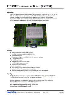
1 USING I2C with PICAXE revolutionRevolution Education Ltd. Email: Web: Version 24/10 :This article provides an introduction into how touse i2c parts with the PICAXE article:1) Describes the i2c bus2) Explains how the i2c bus is used with thePICAXE system3) Gives an example of USING the i2c bus with a24 LCxx series EEPROM4) Gives an example of USING the i2c bus with aDS1307 real time ) Gives an example of USING the i2c bus with aSPE030 speech the information in this datsheet applies to thePICAXE-X parts (18X, 28X, 40X). If you wish toexperiment with use of the i2c bus, we recommenduse of the AXE110 Datalogger fitted with theAXE034 Real Time Clock Upgrade. This will provideyou with a board that has the PICAXE -18X, a24LC16B EEPROM memory chip, and a DS1307real-time-clock chip used in this article.
2 IC- integrated circuit or chip Master- a microcontroller IC that controls the operation of a circuitSlave- a slave IC that does certain specialised tasks for the master ICByte- a number between 0 and 255 Register- a memory location within the slave that stores 1 byte of dataRegister Address- an address that points to a particular memory registerBlock- group of 256 registersEEPROM IC- a slave IC that can store a large amount of dataRTC IC- a slave IC that can maintain the date / time (real-time-clock)ADC IC- a slave IC that can perform analogue-to-digital conversionsSample i2c circuitPICAXE-18X datalogger connections of- 24LC16B EEPROM- DS1307 RTC- SPE030 Speech Module !" #$ % & ' ()%& * % +& & & $( % & (* & % % &$( % ,%- **(.))))
3 ,/ (**% 012 13 4 1556 7 ! 86 2revolutionRevolution Education Ltd. Email: Web: Version 24/10 and the i2c bus What is the i2c bus?The Inter-Integrated-Circuit (i2c) bus was originallydeveloped by Phillips Inc. for the transfer of data betweenICs at the PCB level. The physical interface of thecommunication bus consists of just two lines one for theclock (SCL) and one for the data (SDA). These lines arepulled high by resistors connected to the V+ rail. 4k7 is acommonly used value for these resistors, although theactual value used is not that critical. When either of themaster or slave ICs want to transmit , they pull the lineslow by transistors built inside the IC that controls the bus is called the Master, and is often a microcontroller inthis article a PICAXE -18X microcontroller will be used as the master device.)
4 Theother ICs connected to the bus are called Slaves. There can be more than one slaveon the bus, as long as each slave has been configured to have a unique slaveaddress so that it can be uniquely identified on the bus. In theory there are up toabout 112 different addresses available, but most practical applications wouldgenerally have between 1 and 10 slave use the i2c bus?Advantages: Most major semiconductor manufacturers produce many low-cost i2ccompatible ICs. The range of ICs available is quite extensive - memoryEEPROMs, real-time-clocks, ADCs, DACs, PWM motor/fan controllers, LEDdrivers, digital potentiometers, digital temperature sensors etc. etc. Many of these ICs come in small 8 pin packages.
5 This makes the circuit designvery straight forward. Many slave devices can be connected to the same bus, which only uses two ofthe microcontroller pins. This is a very efficient use of the microcontroller pins. The bus design is very simple, USING just two lines and two : The i2c bus communication protocol is quite complicated. However this can beeasily overcome by USING microcontroller systems such as PICAXE , whichprovide simple BASIC style commands for all the i2c data transfers, andtherefore the end user needs no technical knowledge of the bus communicationprotocols. Each slave IC will have a few unique setup parameters ( slave address), whichmust be extracted from the manufacturers datasheet.
6 This is not normally thatdifficult, once you know the main parameters that you are looking for! ) % * )%* ' % 1 7 % 7 & ' % &()%& *3revolutionRevolution Education Ltd. Email: Web: Version 24/10 and the i2c busSlave Configuration ParametersAlthough all i2c slave devices work in roughly the same way, there are four parametersthat must be checked from the manufacturer s datasheet for each slave device 1 - Slave AddressAs already mentioned, each slave IC on the i2c bus must have a unique address. This isnot generally a problem when USING different types of IC on the same bus, as most ICshave a different default slave slave address is generally 7 bits long, with the 8th bit reserved to indicate whether themaster wishes to write to (1) or read from (0) the slave.
7 A 10-bit slave address is alsopossible, but is rarely used and so not covered in this article. This means the slave addressis often quoted in datasheets as, for instance, 1010000x, with x indicating the read/writebit. When USING the PICAXE system the state of this 8th bit is not important, as thePICAXE system will automatically set or clear the bit as necessary for a read or a it is also possible that you may want to use two or more of the same type of IC( memory EEPROM) on the same bus. This can be overcome by the use of externaladdress pins on the slave device, which can be connected (on the PCB design) to eitherV+ or 0V to give each slave IC on the PCB a unique address. In the case of the popular24 LCxx series of EEPROMs there are 3 external address pins (A2, A1 and A0).
8 Byconnecting these pins to V+ or GND on your circuit design, you can ensure that up to 8parts can be uniquely identified on the same these ICs the datasheet slave address may be quoted as, for instance, 1010dddx, whered is 1 or 0 depending on the state of the external address pin 2 -Bus Speed (100 or 400kHz)The maximum bus speed for data transfer between the master and slave is normally400kHz. However some parts will only work up to 100kHz, and so the manufacturerdatasheet should be checked for each slave IC used. Note this is the maximum speed - allparts can be run at the slower speed if 3 - Register Address Size (Byte or Word)All data transfer from the master to the slave is a write , and this means that a byte of datais transferred from the master to a register within the slave IC.
9 All data transfer from theslave to the master is a read . Simpler slave devices have a maximum of 256 registers, andso a register address of one byte length can be used to identify the particular register ofinterest. However larger devices, particularly memory EEPROMs, have more that 256registers and so may need a word (two byte) register address 4 Page Write BufferAll EEPROM memory chips require a write time to save the data in the chip. This istypically 5 or 10ms. When writing lots of data, this can cause a significant delay. To helpovercome this issue, many ICs have a page write buffer that can accept more than onebyte at once (typically 8, 16 or 32 bytes) so that all these bytes can be programmed atonce.
10 This means, for instance, in the case of 8 bytes you only have one 10ms delay, ratherthan 80ms of delay. Important Note: One of the biggest mistakes made by beginners isthat they don t realise that page writes can only start at a multiple of the buffer size, andcannot overflow the page buffer size. In effect this means (for an 8 byte buffer) you canwrite 8 bytes up from address 0 (or 8 or 16 etc.) but only up 6 bytes from address 2 (10,18 etc.), or else you would overflow the 8 byte page write Education Ltd. Email: Web: Version 24/10 and the i2c bus2) USING i2c with the PICAXE SystemHardwareAll the PICAXE X parts (18X, 28X, 40X) have two pins whichcan be dedicated for the two i2c communication lines SDAand SCL.