Differential high frequency amplifier with
Found 9 free book(s)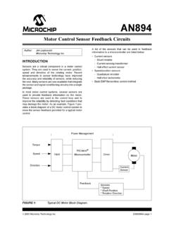
Motor Control Sensor Feedback Circuits
ww1.microchip.comThe high-side shunt circuit requires a high-voltage amplifier that can withstand a high common mode voltage. In addition, the key amplifier specifications are a high CMRR and a low VOS because of the relatively small magnitude of V SENSE. High voltage op amps and integrated differential amplifier ICs are available for systems that have a ...
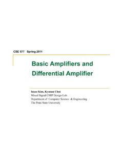
Basic Amplifiers and Differential Amplifier
www.cse.psu.eduBasic Amplifiers: High Frequency Analysis 2/22/2011 Insoo Kim Differential Amplifier Feedback. Fundamentals Definitions DC Operating Point & Load line Large Signal Analysis vs. Small Signal Analysis MOSFET intrinsic Capacitances. Definitions 2/22/2011 Insoo …
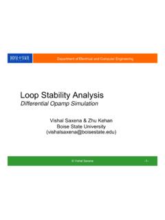
Differential Opamp Simulation
www.eecis.udel.eduvariable is frequency), for a feedback loop or a gain device [1]. ... Unity- gain inverting amplifier transient response with a 200mV differential step (rise/fall time=0.1ns, pulse with=100ns) ... signal analyses followed by PSS is high (e.g. 1G), the maxacfreq parameter (options accuracy) of the PSS can be used to specify the

AD8065/AD8066 (Rev. L) - Analog Devices
www.analog.comperformance. The differential gain and phase errors of 0.02% and 0.02°, respectively, along with 0.1 dB flatness out to 7 MHz, make these amplifiers ideal for video applications. Additionally, they offer a high slew rate of 180 V/µs, excellent distortion (SFDR of −88 dBc @ 1 MHz), extremely high common-mode rejection
Low-noise JFET quad operational amplifier
www.st.comdifferential voltage range • Low input bias and offset current • Low noise en = 15 nV/ √ Hz (typ) • Output short-circuit protection • High input impedance JFET input stage • Low harmonic distortion: 0.01% (typical) • Internal frequency compensation • Latch up free operation • High slew rate: 16 V/µs (typical) Related products

LF353-NWide Bandwidth Dual JFET Input Operational Amplifier
www.ti.comDifferential Input Voltage ±30V Input Voltage Range(4) ±15V ... both inputs exceed the limit, the output of the amplifier will be forced to a high state. ... to the input to minimize “pick-up” and maximize the frequency of the feedback pole by minimizing the. LF353-N.
LC Filter Design (Rev. A) - Texas Instruments
www.ti.coma high level of flexibility for the end application. 1.1 Bridged-Tied Load (BTL) Bridge-tied load (BTL) is the most common output configuration for a class-D amplifier. A BTL configuration consists of one amplifier driving one side of a load and another amplifier, with an inverted signal from the first amplifier, driving the other side of the load.

Low Cost, DC to 500 MHz, 92 dB Logarithmic Amplifier Data ...
www.analog.comComplete multistage logarithmic amplifier 92 dB dynamic range: −75 dBm to +17 dBm to −90 dBm using matching network Single supply of 2.7 V minimum at 7.5 mA typical DC to 500 MHz operation, ±1 dB linearity Slope of 25 mV/dB, intercept of −84 dBm Highly stable scaling over temperature Fully differential dc-coupled signal path
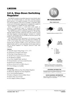
LM2596 - 3.0 A, Step-Down Switching Regulator
www.onsemi.comNORMALIZED FREQUENCY (%) TJ, JUNCTION TEMPERATURE (°C) Figure 8. Standby Quiescent Current Vin, INPUT VOLTAGE (V) Figure 9. Switch Saturation Voltage Figure 10. Switching Frequency Figure 11. Minimum Supply Operating Voltage Figure 12. Feedback Pin Current TJ = 25°C 200 180 140 120 100 80 60 40 20 0 1.6 1.4 1.2 1.0 0.8 0.6 0.4 0.2 5.0 4.5 3.5 ...