ADRV9026 System Development User Guide (Rev. PrA)
The ADRV9026 is designed to operate over the wide frequency ranges of 650 MHz to 6 GHz. The receiver channels support bandwidth up to 200 MHz with data transfer across (up to) four JESD204B/JESD204C lanes at rates up to 16.22 Gbps. The transmitter channels operate over the same frequency range as the receivers.
Download ADRV9026 System Development User Guide (Rev. PrA)

Information
Domain:
Source:
Link to this page:
Documents from same domain

AD743 Ultralow Noise BiFET Op Amp Data Sheet …
www.analog.comREV. E Information furnished by Analog Devices is believed to be accurate and reliable. However, no responsibility is assumed by Analog Devices for its

MT-070: In-Amp Input RFI Protection - Analog …
www.analog.comRev.0, 10/08, WK Page 1 of 6 MT-070 TUTORIAL In-Amp Input RFI Protection . PROTECTING IN-AMPS AGAINST RFI . Real-world applications must deal with an ever increasing amount of radio frequency

LTC3108 - Ultralow Voltage Step-Up Converter and …
www.analog.comLTC3108 3108fc For more information www.linear.com/LTC3108 LDO

1.8 V Low Power CMOS Rail-to-Rail Input/Output …
www.analog.com1.8 V Low Power CMOS Rail-to-Rail Input/Output Operational Amplifier Data Sheet AD8515 Rev. E Document Feedback Information furnished by Analog Devices is believed to be accurate and reliable.

Low Cost Micropower, Low Noise CMOS Rail-to …
www.analog.comLow Cost Micropower, Low Noise CMOS Rail-to-Rail, Input/Output Operational Amplifiers Data Sheet AD8613/AD8617/AD8619 Rev. H Document Feedback Information furnished by Analog Devices is believed to be accurate and reliable.

Low Cost CMOS, High Speed, Rail-to-Rail Amplifiers
www.analog.comLow Cost CMOS, High Speed, Rail-to-Rail Amplifiers Data Sheet ADA4891-1/ADA4891-2/ADA4891-3/ADA4891-4 Rev. F Document Feedback Information furnished by Analog Devices ...

Zero-Drift, Single-Supply, Rail-to-Rail Input/Output ...
www.analog.comZero-Drift, Single-Supply, Rail-to-Rail Input/Output Operational Amplifier Data Sheet AD8628/AD8629/AD8630 FEATURES Lowest auto-zero amplifier noise Low offset voltage: 1 µV AD8628

FEATURES DESCRIPTIO U - analog.com
www.analog.com1 LT1025 1025fb DESCRIPTIO U APPLICATIO S U 80µA Supply Current 4V to 36V Operation 0.5°C Initial Accuracy (A Version) Compatible with Standard Thermocouples (E, J, K, R, S, T) Auxiliary 10mV/°C Output Available in 8-Lead PDIP and SO Packages Thermocouple Cold Junction Compensator Centigrade Thermometer Temperature …

LT1173 - Micropower DC/DC Converter Adjustable …
www.analog.comLT1173 1 Micropower DC/DC Converter Adjustable and Fixed 5V, 12V VOUT 5V/DIV 0V PROGRAM 5V/DIV 5ms/DIV 1173 TA02 L1* 100µH LT1173 • TA01 + GND SW2 FB SW1 ILIM VIN 10 F LT1173

AD9850 CMOS, 125 MHz Complete DDS …
www.analog.comrev. h a cmos, 125 mhz complete dds synthesizer ad9850 functional block diagram clock out clock out analog in analog out dac rset …
Related documents

Integrated, Dual RF Transceiver with Observation Path Data ...
www.analog.comCenter Frequency 300 6000 MHz Tx Large Signal Bandwidth (BW) 100 MHz Tx Synthesis BW2 250 MHz Wider bandwidth for use in digital processing algorithms BW Flatness ±0.5 dB 250 MHz BW, compensated by programmable finite infinite response (FIR) filter ±0.15 dB Any 20 MHz BW span, compensated by programmable FIR filter

Understanding and Performing MIPI D-PHY Physical Layer ...
download.tek.comfrequency will not alter the signal rise time or fall time for both the speed of operations. The measurement algorithm is capable of tolerating the Glitch as shown in Figure 4 when you operate in the broadcast mode and are still able to perform the measurement by selectively qualifying the HS entry mode. Figure 4. Pinpoint triggering.
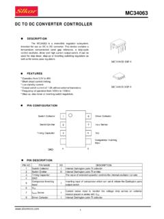
DC TO DC CONVERTER CONTROLLER
atta.szlcsc.comThe MC34063 is a monolithic regulator subsystem, intended for use as DC to DC converter. This device contains a temperature compensated band gap reference, a duty-cycle control oscillator, driver and high current output switch. It can be used for step down, step-up or inverting switching regulators as well as for series pass regulators. FEATURES
LPC546xx Product data sheet
www.nxp.comWatchdog Oscillator (WDTOSC) with a frequency range of 6 kHz to 1.5 MHz. 32.768 kHz low-power RTC oscillator. System PLL allows CPU operation up to the maximum CPU rate and can run from the main oscillator, the internal FRO, the watchdog oscillator or the 32.768 KHz RTC oscillator. Two additional PLLs for USB clock and audio subsystem.
NI 6259 Device Specifications - National Instruments
www.ni.comTiming resolution 50 ns Timing accuracy 50 ppm of sample rate Input coupling DC Input range ±0.1 V, ±0.2 V, ±0.5 V, ±1 V, ±2 V, ±5 V, ±10 V Maximum working voltage for analog inputs (signal + common mode) ±11 V of AI GND CMRR (DC to 60 Hz) 100 dB Input impedance Device on AI+ to AI GND >10 GΩ in parallel with 100 pF

MPC5748G, MPC5748G Microcontroller Data Sheet
www.nxp.com– 96 Configurable Enhanced Modular Input Output Subsystem (eMIOS) channels • Device/board boundary Scan testing supported with per Joint Test Action Group (JTAG) of IEEE (IEEE 1149.1) and 1149.7 (cJTAG) • Security – Hardware Security Module (HSMv2)

ESP32C3 Family
www.mouser.com• A Bluetooth LE subsystem that supports features ... 16 Frequency 30 17 TX Power with Spectral Mask and EVM Meeting 802.11 Standards 30 18 TX EVM Test 30 ... 5 ESP32-C3 Family Power-up and Reset Timing 12 6 Setup and Hold Times for the Strapping Pin 13 7 Address Mapping Structure 16 8 QFN32 (5×5 mm) Package 36 ...