Bipolar Transistor
bipolar transistor models are introduced, i.e. , Ebers–Moll model, small-signal model, and charge control model. Each model has its own areas of applications. he bipolar junction transistor or BJT was invented in 1948 at Bell Telephone Laboratories, New Jersey, USA. It was the first mass produced transistor,
Download Bipolar Transistor

Information
Domain:
Source:
Link to this page:
Documents from same domain
MOS Transistor - Chenming Hu
www.chu.berkeley.eduModern MOSFET technology has advanced continually since its beginning in the 1950s. Figure 6–5 is a transmission electron microscope view of a part of a MOSFET. It shows the poly-Si gate and the single-crystalline Si body with visible individual Si atoms and a 1.2 nm amorphous SiO 2 film between them. 1.2 nm is the size of four SiO 2 molecules.

Device Fabrication Technology1 - Chenming Hu
www.chu.berkeley.edustarting material. A large wafer fab can process 40,000 silicon wafers into circuits each month. The simple example of the device fabrication process shown in Fig. 3–1 includes (a) formation of an SiO 2 layer, (b) its selective removal, (c) introduction of dopant atoms into the wafer surface, and (d) dopant diffusion into silicon. VLSI! ULSI!
MOS Capacitor - Chenming Hu
www.chu.berkeley.edu1.5 nm. One nanometer is equal to 10 Å, or the size of a few oxide molecules. Before 1970, the gate was typically made of metals such as Al (hence the M in MOS). After 1970, heavily doped polycrystalline silicon (see the sidebar, Three Kinds of Solid, in Section 3.7) has been the standard gate material because of its ability to

MOSFETs in ICs—Scaling, Leakage, and Other Topics
www.chu.berkeley.eduThe electron and hole mobility can be raised (or lowered) by carefully engineered mechanical strains. The strain changes the lattice constant of the silicon crystal and therefore the E–k relationship through the Schrodinger’s wave equation. The E–k relationship, in turn, determines the effective mass and the mobility.
Electrons and Holes in Semiconductors
www.chu.berkeley.eduevery silicon atom has four other silicon atoms as its nearest neighbor atoms. This fact is illustrated in Fig. 1–2 with the darkened cluster of a center atom having four neighboring atoms. This cluster is called the primitive cell. Silicon is a group IV element in the periodic table and has four valence electrons. These four electrons
PN and Metal–Semiconductor Junctions
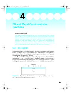
www.chu.berkeley.edu4.1 Building Blocks of the PN Junction Theory 93 (4.1.2) The built-in potential is determined by N a and N d through Eq. (4.1.2). The larger the N a or N d is, the larger the φbi is.Typically, φbi is about 0.9 V for a silicon PN junction. Since a lower E c means a higher voltage (see Section 2.4), the N side is at a higher voltage or electrical potential than the P side.
Motion and Recombination of Electrons and Holes
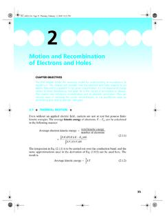
www.chu.berkeley.educollisions is typically 10–13s or 0.1 ps (picosecond), and the distance between collisions is a few tens of nanometers or a few hundred angstroms. The net thermal velocity (averaged over time or over a large number of carriers at any given time) is zero. Thus, thermal motion does not create a steady electric current, but it does introduce a
Related documents

Power MOSFET Basics
www.aosmd.comturn-on of the parasitic bipolar transistor. When no bias is applied to the Gate, the Power MOSFET is capable of supporting a high Drain voltage through the reverse-biased P-body and N- Epi junction. In high voltage devices, most of the ... Gate charge parameter can be used to estimate switching times

Insulated Gate Bipolar Transistor (IGBT) Basics
www.ixys.comThe Insulated Gate Bipolar Transistor (IGBT) is a minority-carrier device with high input impedance and large bipolar current-carrying capability. Many designers view IGBT as a device with MOS input characteristics and bipolar output characteristic that is a voltage-controlled bipolar device. To make use of the advantages of both Power

Failure Mechanisms of Insulated Gate Bipolar Transistors ...
www.nrel.govFailure Mechanisms of Insulated Gate Bipolar Transistors (IGBTs) Nathan Valentine, Dr. Diganta Das, and Prof. Michael Pecht www.calce.umd.edu Center for Advanced Life Cycle Engineering (CALCE) 2015 NREL Photovoltaic Reliability Workshop diganta@umd.edu calce

CHAPTER 2 SINGLE PHASE PULSE WIDTH MODULATED …
www.tntech.edu2.3.1 SPWM With Bipolar Switching In this scheme the diagonally opposite transistors S11, S22 and S21 and S12 are turned on or turned off at the same time. The output of leg A is equal and opposite to the output of leg B. The output voltage is determined by comparing the control signal,

Design And Application Guide For High Speed MOSFET Gate ...
www.radio-sensors.segate drive circuits for high speed switching applications. It is an informative collection of topics offering ... years before the bipolar transistor. The first signal level FET transistors were built in the late 1950’s while power MOSFETs have been available from the mid 70’s. Today, millions of
Writing Simple Spice Netlists - GUC
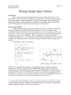
eee.guc.edu.egBipolar Junction Transistor (BJT) Component A bipolar junction transistor is described by QXXXXXXX NC NB NE <NS> MNAME <AREA> <OFF> <IC=VBE, VCE> <TEMP=T> The parameters are: NC I= the name of the collector terminal NB = the name of the base terminal NE = the name of the emitter terminal <NS> = the name of the substrate terminal (optional)

Power MOSFET Basics: Understanding the Turn-On Process
www.vishay.comUnlike bipolar juncti on transistors, these are majority carrier devices. One does not have to worry about current gain, tailoring the base current to match the extremes of hfe and variable collector currents, or providing negative drives. Since ... Fig. 5 - Gate Capacitances with Initial Voltages Fig. 6 - Simplified Inductive Turn-On Circuit ...
IGBT/MOSFET Gate Drive Optocoupler
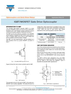
www.vishay.comThe Insulated Gate Bipolar transistor (IGBT) is a cross between a MOSFET (metal oxide semiconductor field effect transistor) and a BJT (bipolar junction transistor) since it combines the positive aspects of MOSFETs and BJTs. The IGBT has …