Bipolar Transistor - Chenming Hu
294 Chapter 8 Bipolar Transistor τB and D B are the recombination lifetime and the minority carrier (electron) diffusion constant in the ba se, respectively. The boundary conditions are [Eq. (4.6.3)] (8.2.3) (8.2.4) where nB0 = ni 2/N B, and NB is the base doping concentration.VBE is normally a forward bias (positive value) and VBC is a reverse bias (negative value).
Download Bipolar Transistor - Chenming Hu

Information
Domain:
Source:
Link to this page:
Documents from same domain
MOS Transistor - Chenming Hu
www.chu.berkeley.eduModern MOSFET technology has advanced continually since its beginning in the 1950s. Figure 6–5 is a transmission electron microscope view of a part of a MOSFET. It shows the poly-Si gate and the single-crystalline Si body with visible individual Si atoms and a 1.2 nm amorphous SiO 2 film between them. 1.2 nm is the size of four SiO 2 molecules.

Device Fabrication Technology1 - Chenming Hu
www.chu.berkeley.edustarting material. A large wafer fab can process 40,000 silicon wafers into circuits each month. The simple example of the device fabrication process shown in Fig. 3–1 includes (a) formation of an SiO 2 layer, (b) its selective removal, (c) introduction of dopant atoms into the wafer surface, and (d) dopant diffusion into silicon. VLSI! ULSI!

MOS Capacitor - Chenming Hu
www.chu.berkeley.edu1.5 nm. One nanometer is equal to 10 Å, or the size of a few oxide molecules. Before 1970, the gate was typically made of metals such as Al (hence the M in MOS). After 1970, heavily doped polycrystalline silicon (see the sidebar, Three Kinds of Solid, in Section 3.7) has been the standard gate material because of its ability to

MOSFETs in ICs—Scaling, Leakage, and Other Topics
www.chu.berkeley.eduThe electron and hole mobility can be raised (or lowered) by carefully engineered mechanical strains. The strain changes the lattice constant of the silicon crystal and therefore the E–k relationship through the Schrodinger’s wave equation. The E–k relationship, in turn, determines the effective mass and the mobility.
Electrons and Holes in Semiconductors
www.chu.berkeley.eduevery silicon atom has four other silicon atoms as its nearest neighbor atoms. This fact is illustrated in Fig. 1–2 with the darkened cluster of a center atom having four neighboring atoms. This cluster is called the primitive cell. Silicon is a group IV element in the periodic table and has four valence electrons. These four electrons
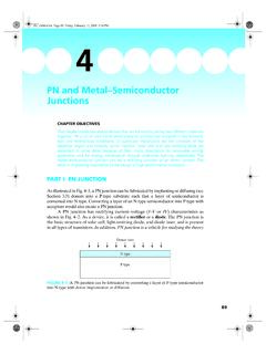
PN and Metal–Semiconductor Junctions
www.chu.berkeley.edu4.1 Building Blocks of the PN Junction Theory 93 (4.1.2) The built-in potential is determined by N a and N d through Eq. (4.1.2). The larger the N a or N d is, the larger the φbi is.Typically, φbi is about 0.9 V for a silicon PN junction. Since a lower E c means a higher voltage (see Section 2.4), the N side is at a higher voltage or electrical potential than the P side.
Motion and Recombination of Electrons and Holes
www.chu.berkeley.educollisions is typically 10–13s or 0.1 ps (picosecond), and the distance between collisions is a few tens of nanometers or a few hundred angstroms. The net thermal velocity (averaged over time or over a large number of carriers at any given time) is zero. Thus, thermal motion does not create a steady electric current, but it does introduce a
Related documents

BJT Amplifiers 6 - Pearson
www.pearsonhighered.comsistor (BJT) circuits are used as small-signal amplifiers. The term small-signal refers to the use of signals that take up a relatively small percentage of an amplifier’s operational range. Additionally, you will learn how to reduce an ampli-fier to an equivalent dc and ac circuit for easier analysis, and you will learn about multistage ...

CIRCUITS LABORATORY EXPERIMENT 6
classes.engineering.wustl.eduFigure 6.7: Hybrid-π model for BJT. In this equivalent circuit, rbb, ree, and rcc represent the ohmic resistance of each region. Thus, rbb is the resistance of the thin base region, ree is the resistance of the emitter region, etc. Typical values of these ohmic resistances are:
CHAPTER 3 Frequency Response of Basic BJT and MOSFET ...
users.encs.concordia.caamplifiers implemented using BJT or MOSFET. 3.3 Simplified high-frequency ac equivalent circuits for BJT and MOSFET devices It can be noted that for amplifiers implemented in integrated circuit technology only the upper cut-off frequency wH,

Section 5.4 – BJT Circuits at DC - ITTC
www.ittc.ku.edu12/3/2004 section 5_4 BJT Circuits at DC 1/1 Jim Stiles The Univ. of Kansas Dept. of EECS Section 5.4 – BJT Circuits at DC Reading Assignment: pp. 421-436 To analyze a BJT circuit, we follow the same boring procedure as always: ASSUME, ENFORCE, ANALYZE

Chapter 5 BJT Biasing Circuits - BU
www.bu.edu.egFigure 5.19 (a) with the thevenin equivalent circuit shown in Figure 5.19 (b). Apply Thevenin’s theorem to the circuit left of point A, with V CC replaced by a short to ground and the transistor disconnected from the circuit. The voltage at point A with respect to ground is and the resistance is

Lecture #4 BJT AC Analysis - BU
www.bu.edu.egBJT Transistor Modeling 5 • the ac equivalent of a transistor network is obtained by: 1. Setting all dc sources to zero and replacing them by a short-circuit equivalent 2. Replacing all capacitors by a short-circuit equivalent 3. Removing all elements bypassed by the short-circuit equivalents introduced by steps 1 and 2 4.

Lesson #12 Small Signal Equivalent Circuits for the BJT
web.njit.eduSmall Signal Equivalent Circuits and Parameters for the BJT rπ-β Model • When the AC Portion of the input is small around the Q point (<< V T in value) then we can approximate the operation of transistor by an equivalent circuit consisting of a resistor, rπ =V T /I BQ and a current source, βi b, where i b is the small signal component of ...

Common Base BJT Amplifier Common Collector BJT Amplifier
www.seas.upenn.eduCommon Base BJT Amplifier ... Equivalent Circuits <=> vout vout V CC /2 Rb R B=R 1∥R 2. ESE319 Introduction to Microelectronics 2008 Kenneth R. Laker (based on P. V. Lopresti 2006) updated 01Oct08 KRL 7 Multisim Bias Check Identical results – as expected! <=>