
Chapter 9 Metal-Semiconductor Contacts
Semiconductor Devices for Integrated Circuits (C. Hu) Slide 9-6 Schottky barrier heights of metal silicide on Si Silicide-Si interfaces are more stable than metal-silicon interfaces. After metal is deposited on Si, an annealing step is applied to form a silicide-Si contact. The term metal-silicon contact includes silicide-Si contacts.
Download Chapter 9 Metal-Semiconductor Contacts

Information
Domain:
Source:
Link to this page:
Documents from same domain
Diodes and Transistors
inst.eecs.berkeley.eduDiodes and Transistors 1. ... basic semiconductor physics. We won’t discuss the details because the point of this ... switch. Below the specified ...
HSPICE Tutorial - University of California, Berkeley
inst.eecs.berkeley.eduHSPICE Tutorial Contents 1 Introduction 1 ... ee105 spice tutorial example 1 - simple rc circuit in the Results Browser and double-clicking vs and vo to plot them in the graph. You may have been able to guess from the netlist, but you’ll see that vsis a …
Introduction to LabVIEW - University of California, …
inst.eecs.berkeley.eduIntroduction to LabVIEW 1. Introduction Welcome to the LabVIEW component of EE100! This lab is just a simple introduction to the graphical circuit simulation ...
Introduction to LabVIEW For Use in Embedded …
inst.eecs.berkeley.eduUC Berkeley EE249 Hugo.Andrade@ni.com Introduction to LabVIEW For Use in Embedded System Development
EE105 –Fall 2015 Microelectronic Devices and Circuits
inst.eecs.berkeley.eduSummary of MOS Single-Transistor Amplifiers MOS Common Source Common Source with Deg. Common Drain Common Gate Ri ∞ ∞ ∞ Small Ro Large Very Large Small Large
Introduction to Digital Systems - University of …
inst.eecs.berkeley.eduDepartment of EECS EE100/42-43 Spring 2007 Rev. 1 Introduction to Digital Systems 0. Acknowledgments Many thanks to Prof. Bernhard Boser and National Instruments for funding this project in the
EE126: Probability and Random Processes - Lecture 1 ...
inst.eecs.berkeley.eduprobability 4 The probabilities summed over all of the base outcomes always equals 1 Example: Toss a fair coin twice 1 Base outcomes are HH,HT,TH,TT 2 This covers all the possibilities. M.E. 3 Each of these outcomes is equally likely 4 Assign each outcome a probability of 0:25. The list (set) of base outcomes is called the Sample Space.
EECS 126 Probability and Random Processes: Course Syllabus ...
inst.eecs.berkeley.eduDescription: Probability is a mathematical discipline that allows one to reason about uncertainty: it helps us to predict uncertain events, to make better decisions under uncertainty, and to design and build systems. Throughout the course, we will teach you the fundamental ideas of probability and random processes along with the labs.
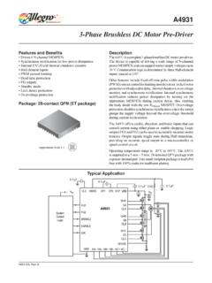
3-Phase Brushless DC Motor Pre-Driver
inst.eecs.berkeley.eduDescription The A4931 is a complete 3-phase brushless DC motor pre-driver . The device is capable of driving a wide range of N-channel power MOSFETs and can support motor supply voltages up to
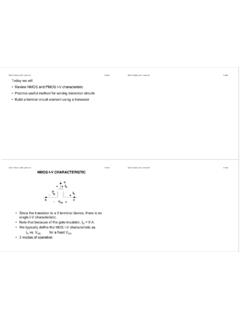
DS -V I G - EECS Instructional Support Group Home Page
inst.eecs.berkeley.eduG D S I D I G-V DS + + V G S _ NMOS I-V CHARACTERISTIC • Since the transistor is a 3-terminal device, there is no single I-V characteristic. • Note that because of the gate insulator, I G = 0 A. • We typically define the MOS I-V characteristic as I D vs. V DS for a fixed V GS. • 3 modes of operation
Related documents

SEMICONDUCTOR MEMORIES
bwrcs.eecs.berkeley.eduSemiconductor Memory Classification RWM NVRWM ROM EPROM E2PROM FLASH Random Access Non-Random Access SRAM DRAM Mask-Programmed Programmable (PROM) FIFO Shift Register CAM ... Metal bypass K cells Polysilicon word line WL Polysilicon word line Driver (b) Using a metal bypass (a) Driving the word line from both sides Metal word line WL
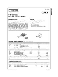
FQP30N06L 60V LOGIC N-Channel MOSFET
cdn.sparkfun.com©2001 Fairchild Semiconductor Corporation Rev. A1. May 2001 0 5 10 15 20 25 30 0 2 4 6 8 10 12 V DS = 30V V DS = 48V ※ Note : I D = 32A V GS, Gate-Source Voltage [V] Q G, Total Gate Charge [nC] 10-1 100 101 0 500 1000 1500 2000 C iss = C gs + C gd (C ds = shorted) C oss = C ds + C gd C rss = C gd ※ Notes : 1. V GS = 0 V 2. f = 1 MHz C rss ...

Metal/Semiconductor Ohmic Contacts - Stanford University
web.stanford.eduis a constant dependent upon metal and the semiconductor. Specific contact resistivity, ρ c primarily depends upon • the metal-semiconductor work function, φΒ, • doping density, N, in the semiconductor and • the effective mass of the carrier, m*.

AppCompendium Semiconductor ICP-MS-5991-9495EN-US …
www.agilent.comMay 01, 2012 · Agilent ICP-MS Solutions for the Semiconductor Industry 8 Automating Analysis of Metal Contaminants in Si Wafers 9 Setups for Different Sample Types 11 Expanding Capabilities with Accessories and Software 15 Online Monitoring of Metal Contaminants in Process Chemicals 16 Contamination Control 17 ICP-MS Applications 18 Cleaning/Etching 19

Marking Transition Brochure ON Semiconductor Part
www.electro-tech-online.comOn August 5th, 1999 Motorola's former Semiconductor Components Group emerged as ON Semiconductor, an independent company focused on standard discrete, logic and analog semiconductor products. As part of the terms of separation ON Semiconductor was granted the ability to manufacture and sell Motorola logo-marked products for one year.

Introduction to Semiconductor Technology ...
www.st.comINTRODUCTION TO SEMICONDUCTOR TECHNOLOGY 2 BASIC IC ELEMENT: THE TRANSISTOR 2.1 MOS TECHNOLOGY We will examine first the basics of MOS (Metal Oxide Semiconductor) technologies as they are used for the majority of the integrated circuits manufactured at STMicroelectronics.

Metal Can Packages (TO-3/5/8/18/39/46/52/72)
www.ti.comNational Semiconductor Corporation Americas Tel: 1-800-272-9959 Fax: 1-800-737-7018 Email: support@nsc.com National Semiconductor Europe Fax: +49 (0) 1 80-530 85 86 Email: europe.support@nsc.com Deutsch Tel: +49 (0) 1 80-530 85 85 English Tel: +49 (0) 1 80-532 78 32 Français Tel: +49 (0) 1 80-532 93 58 Italiano Tel: +49 (0) 1 80-534 16 80 ...