CMOS Manufacturing Process
Etch and fill trenches Implant well regions Deposit and pattern polysilicon layer Implant source and drain regions and substrate contacts Create contact and via windows Deposit and pattern metal layers. Digital Integrated Circuits Manufacturing Process …
Download CMOS Manufacturing Process

Information
Domain:
Source:
Link to this page:
Documents from same domain
chapter2.fm Page 33 Monday, September 4, 2000 …
bwrcs.eecs.berkeley.eduIC packaging Future Trends in Integrated Circuit Technology 2.1 Introduction 2.2 Manufacturing CMOS Integrated Circuits 2.2.1 The Silicon Wafer 2.2.2 Photolithography 2.2.3 Some Recurring Process Steps ... cess that lies at the core of the semiconductor revolution. Yet, some insight in the steps ...

Designing a Divider - University of California, Berkeley
bwrcs.eecs.berkeley.eduDigital Integrated Circuits 2/e DIVIDE HARDWARE Version 1 ° 64-bit Divisor reg, 64-bit ALU, 64-bit Remainder reg, 32-bit Quotient reg Remainder Quotient Divisor …
Lecture 9: Digital Signal Processors: Applications and ...
bwrcs.eecs.berkeley.eduProcessor Applications General Purpose - high performance ... Digital camera - TMS320C5000 ... DSP evolved from Analog Signal Processors, using analog hardware to transform phyical signals (classical electrical engineering) ASP to DSP because

DESIGNING COMBINATIONAL LOGIC GATES IN CMOS
bwrcs.eecs.berkeley.edu198 DESIGNING COMBINATIONAL LOGIC GATES IN CMOS Chapter 6 6.1Introduction The design considerations for a simple inverter circuit ere presented in the previousw chapter. In this chapter, the design of the inverter will be extended to address the synthesis

DESIGNING SEQUENTIAL LOGIC CIRCUITS
bwrcs.eecs.berkeley.edu272 DESIGNING SEQUENTIAL LOGIC CIRCUITS Chapter 7 7.1 Introduction Combinational logic circuits that were described earlier have the property that the output

Lecture11-MOS Cap Delay
bwrcs.eecs.berkeley.eduEE141 25 EECS141 Lecture #11 25 The Miller Effect V in M1 C gd1 V out ∆V As V in increases, V out drops – Once get into the transition region, gain from V in to V out > 1 So, C gd experiences voltage swing larger than V
Chapter 4 Calculating the Logical Effort of Gates
bwrcs.eecs.berkeley.edu4.3 Calculating logical effort Definition 4.2 provides a convenient method for calculating the logical effort of a logic gate. We have but to design a gate that has the same current drive character-istics as a reference inverter, calculate the input capacitances of each signal, and apply Equation 4.1 to obtain the logical effort.

DESIGNING COMBINATIONAL LOGIC GATES IN CMOS
bwrcs.eecs.berkeley.eduof arbitrary digital gates such as NOR, NAND and XOR. The focus will be on combina-tional logic (or non-regenerative) circuits that have the property that at any point in time, the output of the circuit is related to its current input signals by some Boolean expression (assuming that the transients through the logic gates have settled).
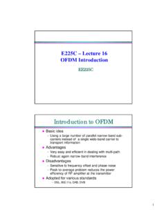
Introduction to OFDM
bwrcs.eecs.berkeley.eduOFDM Introduction EE225C Introduction to OFDM lBasic idea ... – Selective Fading – Very short pulses – ISI iscompartively long – EQs are then very long – Poor spectral efficiency because of band guards Drawbacks ... 2 4 6 8 10 12 14 16-60-55-50-45-40-35-30-25-20-15-10

SEMICONDUCTOR MEMORIES
bwrcs.eecs.berkeley.eduThe read-out of the 1T DRAM cell is destructive; read and refresh operations are necessary for correct operation. Unlike 3T cell, 1T cell requires presence of an extra capacitance that must be explicitly included in the design. When writing a “1” into a DRAM cell, a threshold voltage is lost.
Related documents
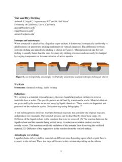
Wet and Dry Etching - University of California, Davis
www.ece.ucdavis.eduetch rate. Silicon dioxide or silicon nitride is usually used as a masking material against HNA. As the reaction takes place, the material is removed laterally at a rate similar to the speed of etching downward. This lateral and downward etching process takes places even with isotropic dry etching which is described in the dry etch section.
Etch rates for micromachining processing-part II ...
www.seas.upenn.eduthe etch rates of other materials that will be exposed to the etch, such as masking films and underlying layers, enables an etch process to be chosen for good selectivity (high ratio of etch rate of the target material to etch rate of the other material)—if one exists. While several large literature-review compilations
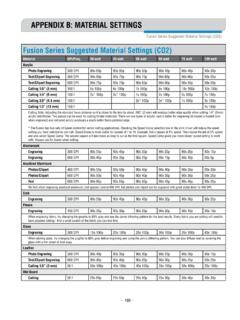
APPENDIX B: MATERIAL SETTINGS - Epilog Laser
www.epiloglaser.comis very narrow. If the application calls for a black etch, consider using an oxidizer after engraving. Oxidizers are used most commonly if the aluminum has a protective coating (urethane, clear coat, clear anodized) covering the area that is not engraved. Deep metal engraving on aluminum can be done using multiple passes.
Radiofrequency Plasma Sources for Semiconductor Processing
www.seas.ucla.edu1 2 3 4 5 6 7 8 9 10 11 12 13 14 15 16 17 18 19 20 21 22 23 24 25 26 27 28 29 30 31 32 33 34 35 36 37 38 39 40 41 42 43 44 45 Thisisusuallyatalowerfrequency ...
Chapter 1.10 - Miscellaneous Etchants
nanolab.berkeley.eduetch oxide, it is important to remember to dip off any native oxide from the silicon surfaces to be etched in HF solution. Etch rates and temperatures are given below. Complete instructions on the use of EDP are given in Chapter 1.3 of the lab manual. Ethylenediamine N H. 2: