
DESIGNING COMBINATIONAL LOGIC GATES IN CMOS
In Figure 6.6b, the subnets (SN) for the pull-down etwork aren identified t the topA level, SN1 and SN2 are in parallel so in the dual network, they will be in series. Since SN1 B A A B Parallel Combination Figure 6.4 NMOS logic ules r — series devices implement an AND, and parallel devices implement an OR. (a) series (b) parallel Series ...
Download DESIGNING COMBINATIONAL LOGIC GATES IN CMOS
Information
Domain:
Source:
Link to this page:
Documents from same domain
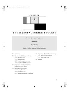
chapter2.fm Page 33 Monday, September 4, 2000 …
bwrcs.eecs.berkeley.eduIC packaging Future Trends in Integrated Circuit Technology 2.1 Introduction 2.2 Manufacturing CMOS Integrated Circuits 2.2.1 The Silicon Wafer 2.2.2 Photolithography 2.2.3 Some Recurring Process Steps ... cess that lies at the core of the semiconductor revolution. Yet, some insight in the steps ...

Designing a Divider - University of California, Berkeley
bwrcs.eecs.berkeley.eduDigital Integrated Circuits 2/e DIVIDE HARDWARE Version 1 ° 64-bit Divisor reg, 64-bit ALU, 64-bit Remainder reg, 32-bit Quotient reg Remainder Quotient Divisor …
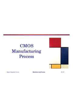
CMOS Manufacturing Process
bwrcs.eecs.berkeley.eduDigital Integrated Circuits Manufacturing Process EE141 A Modern CMOS Process p-well n-well p+ p-epi SiO 2 AlCu poly n+ SiO 2 p+ gate-oxide Tungsten TiSi 2 Dual-Well Trench-Isolated CMOS Process
Lecture 9: Digital Signal Processors: Applications and ...
bwrcs.eecs.berkeley.eduProcessor Applications General Purpose - high performance ... Digital camera - TMS320C5000 ... DSP evolved from Analog Signal Processors, using analog hardware to transform phyical signals (classical electrical engineering) ASP to DSP because

DESIGNING SEQUENTIAL LOGIC CIRCUITS
bwrcs.eecs.berkeley.edu272 DESIGNING SEQUENTIAL LOGIC CIRCUITS Chapter 7 7.1 Introduction Combinational logic circuits that were described earlier have the property that the output

Lecture11-MOS Cap Delay
bwrcs.eecs.berkeley.eduEE141 25 EECS141 Lecture #11 25 The Miller Effect V in M1 C gd1 V out ∆V As V in increases, V out drops – Once get into the transition region, gain from V in to V out > 1 So, C gd experiences voltage swing larger than V
Chapter 4 Calculating the Logical Effort of Gates
bwrcs.eecs.berkeley.edu4.3 Calculating logical effort Definition 4.2 provides a convenient method for calculating the logical effort of a logic gate. We have but to design a gate that has the same current drive character-istics as a reference inverter, calculate the input capacitances of each signal, and apply Equation 4.1 to obtain the logical effort.

DESIGNING COMBINATIONAL LOGIC GATES IN CMOS
bwrcs.eecs.berkeley.eduof arbitrary digital gates such as NOR, NAND and XOR. The focus will be on combina-tional logic (or non-regenerative) circuits that have the property that at any point in time, the output of the circuit is related to its current input signals by some Boolean expression (assuming that the transients through the logic gates have settled).
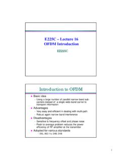
Introduction to OFDM
bwrcs.eecs.berkeley.eduOFDM Introduction EE225C Introduction to OFDM lBasic idea ... – Selective Fading – Very short pulses – ISI iscompartively long – EQs are then very long – Poor spectral efficiency because of band guards Drawbacks ... 2 4 6 8 10 12 14 16-60-55-50-45-40-35-30-25-20-15-10

SEMICONDUCTOR MEMORIES
bwrcs.eecs.berkeley.eduThe read-out of the 1T DRAM cell is destructive; read and refresh operations are necessary for correct operation. Unlike 3T cell, 1T cell requires presence of an extra capacitance that must be explicitly included in the design. When writing a “1” into a DRAM cell, a threshold voltage is lost.
Related documents
Chapter 8 Natural and Step Responses of RLC Circuits
www.ee.nthu.edu.twChapter 8 Natural and Step Responses of RLC Circuits 8.1-2 The Natural Response of a Parallel RLC Circuit. 8.3 The Step Response of a Parallel . RLC . Circuit. 8.4 The Natural and Step Response of a Series . RLC . Circuit
Chapter 12 Alternating-Current Circuits
web.mit.eduFigure 12.2.2 (a) Time dependence of IR (t) and VR (t) across the resistor.(b) Phasor diagram for the resistive circuit. The behavior of IR (t)and can also be represented with a phasor diagram, as shown in Figure 12.2.2(b). A phasor is a rotating vector having the following properties:

DC Electrical Circuit Analysis - MVCC
www2.mvcc.eduSubsequent chapters introduce resistance, series circuits, parallel circuits and series-parallel circuits. The text continues with chapters covering network theorems, more advanced techniques such as nodal and mesh analysis, and finally finishes with introductions to capacitors, inductors and magnetic circuits. The companion AC

Chapter 6: Inductance and Capacitance
courses.egr.uh.eduChapter 6: Inductance and Capacitance We introduce here the two remaining basic circuit elements: the inductor and the capacitor. The behavior of the inductor is based on the properties of the magnetic field generated in a coil of wire. In fact, the inductor is basically a coil of wire. Ampere’s Law: current in a coil magnetic field

A TEXTBOOK OF ELECTRICAL TECHNOLOGY
elbook.weebly.com6. The chapter on Series A.C. Circuits has been enriched with many articles such as Determination of Upper and Lower Half-power Frequencies, Value of Edge Frequencies and Relation between Resonant Power and Off-resonance Power. ... Between Series and Parallel Circuits—Relative Potential— ...
Chapter 6 PROBLEMS - #hayalinikeşfet
home.ku.edu.trThen, each of the pMOS has an output resistance equal to 6.5 k. The output resistance is equal to the series of one of these resistance with the parallel of four of the same resistnaces. Then, the minimum output resistance is 6.5 k + 6.5 k/4 = 8.125 k. 6. [E, None, 4.2] What is the logic function of circuits A and B in Figure 6.5? Which one is a
Chapter 18 Two-Port Circuits
www.ee.nthu.edu.tw1. Chapter 18 Two-Port Circuits. 18.1 The Terminal Equations. 18.2 The Two-Port Parameters. 18.3 Analysis of the Terminated Two-Port Circuit . 18.4 Interconnected Two-Port Circuits

Series -Parallel Circuits
www.oakton.edu6-1: Finding RTfor Series -Parallel Resistances Overview of Series-Parallel Circuits A series-parallel circuit, or combination circuit, combines both series and parallel connections. Most electronic circuits fall into this category. Series-parallel circuits are typically used when different voltage and current values are required from the same

Electric circuits, Current, and resistance (Chapter 22 and 23)
www.physics.brocku.catraded for a 6.0 V battery. The power dissipated by the resistoris now A. 1.0 W B. 2.0 W C. 3.0 W D. 4.0 W Multiple choice Problem 1: An electric blanket has a wire that runs through the interior. A current causes energy to be dissipated in the wire, warming the blanket. A new, low-voltage electric blanket is rated to be used at 18 V.