
GaN HEMTを用いた携帯電話基地局向け 広帯域・高出力・高 …
(GaN HEMT※1: Gallium Nitride High Electron Mobility Transistor)の研究および開発を2000年から進め、2006 ... power wideband asymmetric Doherty amplifier using the devices are also described. The transistor has a pair of 180 W GaN dies. The internal matching circuit is designed with a high-dielectric substrate so that it can ...
Download GaN HEMTを用いた携帯電話基地局向け 広帯域・高出力・高 …

Information
Domain:
Source:
Link to this page:
Documents from same domain

UL規格電線 UL STANDARD ELECTRONIC WIRE UL …
sei.co.jp※本カタログの仕様・構成等は性能改善の為、お断り無く変更する場合がございます。 ※This specification is subject to change without a prior announcement.
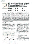
高速(100G/200G/400G 用)高感度APDチップ搭載4ch 集積 …
sei.co.jp80 高速(100g/200g/400g用)高感度apdチップ搭載4ch集積受信デバイス 特集 1. 緒 言 lte※1等の高速な無線ネットワークのサービス ...

PHEV/EV用給電コンバータの開発
sei.co.jp−()78 − phev/ev用給電コンバータの開発 3−3 力率改善回路(pfc)の設計 商用系統の電源 から高圧バッテリに電力を供給する給電コンバータには、

UL, C-UL STANDARD ELECTRONIC WIRE UL STYLE 1283 LF, c …
sei.co.jpSTRENG-TH VAC(1min) 外 径 NOM. DIA. (mm) 導体 Conductor AWG4 材質 Material 材質 Material 構成 Composition 外径 Diameter 絶縁体 Insulation 柔軟性(*1試験方法) Flexibility (*1 test method) 許容電流(雰囲気温度:30℃) Permissible current (Atmosphere:30℃) 低温性 Low-temperature resistance スミ ...
UL規格電線 UL STANDARD ELECTRONIC WIRE UL STYLE 1571 LF
sei.co.jpSTRENG-TH VAC(1min) 外 径 NOM. DIA. (mm) 1571 UL スタイルNo. UL STYLE No. 定 格 RATING 導 体(錫めっき軟銅線) CONDUCTOR (Tinned Annealed Copper Wire) 絶縁体(鉛フリーイラックス® V2) INSULATION (Lead Free IRRAX™V2) 温 度 TEMP. (℃) 80 30 15 500 電 圧 VOLT. (VAC) サイズ SIZE (AWG) 32 30 28 20/0.05 30 ...

電力貯蔵用レドックスフロー電池
sei.co.jpIn particular, a redox flow battery, which is suitable for large scale energy storage, has currently been developed at various organizations around the world. This paper reviews the technical development of the redox flow battery. Keywords: redox flow battery, energy storage, renewable energy, battery, vanadium

半導体量子デバイスの多様な展開 - SEI
sei.co.jpDevelopment of Various Semiconductor Quantum Devices ─by Tsukuru Katsuyama Semiconductor quantum devices, composed of semiconductor quantum wells and superlattices, are widely used in our daily lives as key devices for opto-electronic equipment. The quantum well structure consists of alternating ultra-thin semiconductor
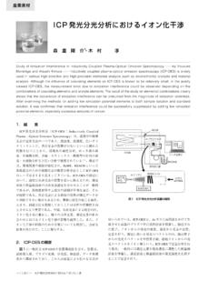
I C P 発光分光分析におけるイオン化干渉 - SEI
sei.co.jpMorishige and Atsushi Kimura─Inductively coupled plasma-optical emission spectroscopy (ICP-OES) is widely used in various high-sensitive and high-precision elemental analysis such as environmental analysis and material analysis. Although the influence of coexisting elements on ICP-OES is known to be relatively small, in the axially

SUPPLEMENTARY DATA 許容電流計算式 PERMISSIBLE …
sei.co.jpη0:Permissible current reduction coefficient in the case of multi-wire installation The conductor resistance r of electronic wire is calculated by the following formula.

機器用電線 イラックス A 絶縁電線 IRRAX A - SEI
sei.co.jpIRRAX™A 優れた耐熱性と高周波特性の点から計算機、測定器類の内部配線 用電線として最適です。イラックス®B電線に比べて柔軟なため、 特に狭い機内配線用電線としておすすめできます。 These wires are used as electronic wires for internal wiring of
Related documents

Transphrom–氮化镓FET(HEMT)
www.dianyuan.comTransphrom–氮化镓FET(HEMT) www.transphormusa.com, HEMT: High Electron Mobility Transistor 氮化镓MOSFET (600VDC, 能承受周期为1uS,100nS的连续的方波,保证750V) Part Number Package Voltage (V) Current (A) Ron(Ohm) Description TPH3245ED下载 QFN 5*6 750 6 0.5 背部金属接D极 TPH3002LD下载 QFN 8*8 750 9 0.29 背部金属 ...

NCP51820 - High Speed Half-Bridge Driver for GaN Power ...
www.onsemi.comDriver for GaN Power Switches NCP51820 The NCP51820 high−speed, gate driver is designed to meet the stringent requirements of driving enhancement mode (e−mode), high electron mobility transistor (HEMT) and gate injection transistor (GIT), gallium nitrade (GaN) power switches in off−line, half−bridge power topologies.
Gallium Nitride (GaN) versus Silicon Carbide (SiC)
www.richardsonrfpd.comGallium Nitride (GaN). These material properties have a major influence on the fundamental performance characteristics of the devices. Both SiC and GaN have material properties superior to Si for RF and Switching Power devices. The high critical field of both GaN and SiC compared to Si is a property which allows these

Insights into gallium oxide growth
data.angel.digitalMar 01, 2022 · the INN40W08, a 40 V bi-directional GaN-on-silicon enhancement mode HEMT for mobile devices, including laptops and cellular phones. The INN40W08 HEMT has been developed using the company’s InnoGaN technology. Denis Marcon, general manager of Innoscience Europe and marketing manager for the USA and Europe, remarked: “GaN …

HEMT - Fujitsu
www.fujitsu.comGaN HEMT I ds V ds 0 0 ドレイン電圧 V ds ( V ) ドレイン電流 I ds ( A ) (b)GaN HEMTとSJ Si MOSFETのパルス応答特性 スイッチング損失 スイッチング損失 表-2 スイッチング特性比較 GaN HEMT Si MOSFET オン時間(ns) 7.0 41.5 オフ時間(ns) 7.5 30.5 オン損失(µJ) 5.6 45.4 ...

GaN系半導体デバイスの技術開発課題と ... - JST
www.jst.go.jpThe GaN devices are expected to be developed for various applications in near future because of the attractive physical properties of GaN including wide bandgap, optical properties and electrical properties. In this report, the current status of the researches and developments of laser diodes, high-frequency ... 5.1 横型HEMT構造と縦型 ...