ICM7555 General purpose CMOS timer
n Wide operating supply voltage range guaranteed 3 V to 16 V over full automotive temperatures n Normal reset function; no crowbarring of supply during output transition ... VI input voltage TRIGGER: VDD = 5 V 0.29VDD 0.31VDD 0.34VDD V CONTROL_VOLTAGE: VDD = 5 V 0.62VDD 0.65VDD 0.67VDD V THRESHOLD: ...
Download ICM7555 General purpose CMOS timer

Information
Domain:
Source:
Link to this page:
Documents from same domain

AN10441 Level shifting techniques in I2C-bus design
www.nxp.comDocument information AN10441 Level shifting techniques in I2C-bus design Rev. 01 — 18 June 2007 Application note Info Content Keywords I2C-bus, level shifting Abstract Logic level shifting may be required when interfacing legacy devices with

AN3234: Washing Machine Three-Phase AC …
www.nxp.comWashing Machine Three-Phase AC Induction Motor Drive, Rev. 0 Indirect Vector Control 4 Freescale Semiconductor If you are looking for more theory on the field ...

1. General description - nxp.com
www.nxp.com1. General description The TJA1044 is part of the Mantis family of high-speed CAN transceivers. It provides an interface between a Controller Area Network (CAN) protocol controller and the physical

PCA9570 Remote 4-bit general purpose outputs for 1 MHz …
www.nxp.com1. General description The PCA9570 is a CMOS device that provides 4 bits of General Purpose parallel Output (GPO) expansion in low voltage processor and handheld battery powered mobile

P82B96 Dual bidirectional bus buffer - nxp.com
www.nxp.com1. General description The P82B96 is a bipolar IC that creates a non-latching, bidirectional, logic interface between the normal I2C-bus and a range of other bus configurations.It can interface

S32K144 EVB Quick Start Guide - NXP Semiconductors
www.nxp.comJ14 SWD connector. 3 EXTERNAL USE S32K144 EVBFeatures: ... USB connector of the USB cable to micro-B port J7 on the S32K144EVB. ... Windows, Linux and Mac operating systems. Using the MSD Flash Programmer 1. Locate the .srec file of your project , file is under the

Three-Phase BLDC Motor Sensorless Control Using …
www.nxp.comThis document describes the design of a three-phase brushless DC motor (BLDC motor) drive based on Freescale’s MC56F8013 and MC56F8023 dedicated motor control device. Brushless DC motors are popular in a wide application area.

AN11443 BFU550XR ISM 433 MHz LNA design - nxp.com
www.nxp.comAN11443 BFU550XR ISM 433 MHz LNA design Rev. 1 — 23 January 2014 Application note . Document information Info Content Keywords BFU520, BFU530, BFU550 series, ISM-band, 433MHz 866MHz Abstract This document describes an ISM Frequency LNA design on BFU5xxXR Starter kit

DSP56156 16-Bit Digital Signal Processor - nxp.com
www.nxp.comThe DSP56156 is a general-purpose MPU-style Digital Signal Processor (DSP). On a single semi- conductor chip, the DSP56156 comprises a very efficient 16-bit digital signal processing core, pro-

SAA7706H Car radio Digital Signal Processor (DSP)
www.nxp.comCar radio Digital Signal Processor (DSP) SAA7706H This text is here in white to force landscape pages to be rotated correctly when browsing through the pdf in the Acrobat reader.This text is here in _white to force landscape pages to be rotated correctly when browsing through the pdf in the Acrobat reader.This text is here inThis text is here in
Related documents
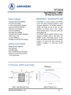
AEROSEMI - Olimex
www.olimex.comInput and Output capacitors should be placed close to the IC and connected to ground plane to reduce noise coupling. The GND should be connected to a strong ground plane for heat sinking and noise protection. Keep the main current traces as possible as short and wide. SW node of DC-DC converter is with high frequency voltage swing.

LF353-NWide Bandwidth Dual JFET Input Operational Amplifier
www.ti.com• Fast Settling Time to 0.01%: 2 μs input offset voltage, low input bias current, high input impedance, high slew rate and wide bandwidth. The devices also exhibit low noise and offset voltage drift. Typical Connection 1 Please be aware that an important notice concerning availability, standard warranty, and use in critical applications of

KAAP686 Mathematics and Signal Processing for …
www1.udel.eduApr 27, 2011 · The rectified signal is low pass filtered, with in the 5 – 100 Hz range, and the result looks like the “envelope” of the original signal. One way to low pass filter a signal is to simply take the mean value, in a window which “slides” along the signal. Some authors advocate this “rectify and mean” approach. Such a moving–average
Analog to Digital Conversion - mccdaq.com
www.mccdaq.cominput of 10 VDC can resolve the measurement into 10 VDC/4096 = 0.00244 VDC = 2.44 mV. Similarly, for the same 0 to 10 VDC range, a 16-bit ADC resolution is 10/216 = 10/65,536 = 0.153 mV. The resolution is usually specified with respect to the full-range reading of the ADC, not with respect to the measured value at any particular instant.
SECTION 4 SWITCHED CAPACITOR VOLTAGE CONVERTERS …
www.analog.comSwitched capacitor voltage converters do not maintain high efficiency for a wide range of ratios of input to output voltages, unlike their switching regulator counterparts. Because the input to output current ratio is scaled according to the basic voltage conversion (i.e., doubled for a doubler, inverted for an inverter)

LM339 - Single Supply Quad Comparators
www.onsemi.com• Low Input Bias Current: 25 nA (Typ) • Low Input Offset Current: ±5.0 nA (Typ) • Low Input Offset Voltage • Input Common Mode Voltage Range to GND • Low Output Saturation Voltage: 130 mV (Typ) @ 4.0 mA • TTL and CMOS Compatible • ESD Clamps on the Inputs Increase Reliability without Affecting Device Operation
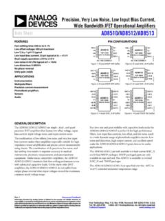
Precision, Very Low Noise, Low Input Bias Current, Wide ...
www.analog.comoutput phase reversal when input voltages exceed the maximum common-mode voltage range. Fast slew rate and great stability with capacitive loads make the AD8510/AD8512/AD8513 a perfect fit for high performance filters. Low input bias currents, low offset, and low noise result in a wide dynamic range of photodiode amplifier circuits. Low

LM2576 - 3.0 A, 15 V, Step-Down Switching Regulator
www.onsemi.com• Adjustable Version Output Voltage Range, 1.23 to 37 V ±4% Maximum Over Line and Load Conditions • Guaranteed 3.0 A Output Current • Wide Input Voltage Range • Requires Only 4 External Components • 52 kHz Fixed Frequency Internal Oscillator • TTL Shutdown Capability, Low Power Standby Mode • High Efficiency