
“L” Matching Networks
ECE145A/ECE218A Impedance Matching Notes set #5 Page 7 Of course, we can also do this quite nicely on the Smith Chart. Series L Shunt C RL Normalize to 50 Ω. Then rp = 10 on real axis. Move on constant conductance circle down + 0.3 to the r = 1 circle (capacitive
Download “L” Matching Networks

Information
Domain:
Source:
Link to this page:
Documents from same domain
Transistor Technologies for High Efficiency and Linearity
web.ece.ucsb.eduDifferential Topology • Double the available voltage swing • Even-order harmonic suppression • Double the frequency of current injection into substrate –Reduce the potential for LO-pulling • The tail current source is removed from the standard differential pair (this is a “quasi-differential” structure) –DC current set by the biasing of input devices

Phase Locked Loop Circuits
web.ece.ucsb.eduClock generation: B. Razavi, Design of Analog CMOS Integrated Circuits, Chap. 15, McGraw-Hill, 2001. 1. Definition. A PLL is a feedback system that includes a VCO, phase detector, and low pass filter within its loop. Its purpose is to force the VCO to replicate and track the frequency and phase at the input when in lock.

ADS Tutorial Stability and Gain Circles ECE145A/218A
web.ece.ucsb.eduequations. The syntax is: gp_circle(S, gain, # points on circle) where S is the S-parameter matrix. Let’s illustrate. In the example below, a table is used to display frequency, maximum stable gain (MSG), the stability factor, k, and the magnitude of delta. The gain circles are at MSG (MaxGain1 in this case), and 1 and 2 dB below MSG.
Audio Amplifier Circuit - UC Santa Barbara
web.ece.ucsb.eduWeek #1: Audio amplifier Week #2: Microphone circuit The audio amplifier project is more difficult and time-consuming than the microphone pre-amp, so part of week #2 may be used to finish the audio amp. All breadboarding and testing can and should be done in lab. Soldering and hardwiring can and should be done outside lab.

Harmonic Balance Simulation on ADS
web.ece.ucsb.eduHarmonic Balance Simulation on ADS General Description of Harmonic Balance in Agilent ADS 1 Harmonic balance is a frequency-domain analysis technique for simulating nonlinear circuits and systems. It is well-suited for simulating analog RF and microwave circuits, ... function is driven to a given small value), then the resulting voltage ...
Quality factor, Q
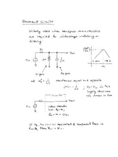
web.ece.ucsb.eduWhen a resonant circuit is connected to the outside world, its total losses (let’s call them RP or GP) are combined with the source and load resistances, RS and RL. For example, Here is a parallel resonant circuit (C,L and RP)connected to the outside. The total Q of this circuit is called the loaded Q or QL and is given by

Latches, the D Flip-Flop & Counter Design
web.ece.ucsb.eduFebruary 6, 2012 ECE 152A - Digital Design Principles 2 Reading Assignment Brown and Vranesic 7Flip-Flops, Registers, Counters and a Simple Processor 7.1 Basic Latch 7.2 Gated SR Latch 7.2.1 Gated SR Latch with NAND Gates 7.3 Gated D …

Flip-Flops and Sequential Circuit Design
web.ece.ucsb.edu11 Latches and Flip-Flops 11.5 S-R Flip-Flop 11.6 J-K Flip-Flop 11.7 T Flip-Flop 11.8 Flip-Flops with Additional Inputs 11.9 Summary 12 Registers and Counters 12.5 Counter Design Using S-R and J-K Flip-Flops 12.6 Derivation of Flip-Flop Input Equations – Summary

BASICS OF THE SPECTRUM ANALYZER - UC Santa Barbara
web.ece.ucsb.eduFourier ⋅ π → − + + Now instead of a bank of narrow filters, we shall have one narrow filter centered at a fixed frequency, say fI, and we shall scan the signal spectrum across this filter by multiplying x(t) by a sinusoid of varying frequency f0. See Figure 1. …

Mealy and Moore Machines
web.ece.ucsb.eduFebruary 22, 2012 ECE 152A - Digital Design Principles 5 Finite State Machines Two types (or models) of sequential circuits (or finite state machines) Mealy machine Output is function of present state and present input Moore machine Output is function of present state only Analysis first, then proceed to the design of
Related documents

RF, Microwave, and Millimeter Wave Products Selection …
www.analog.comADL8111: 10 MHz to 8 GHz Switchable Bypass Wideband LNA 17 Gain Blocks and Driver Amplifiers 18 Low Phase Noise Amplifiers 19 Wideband Distributed Amplifiers 20 Linear and Power Amplifiers 21 ADPA9002: GaAs pHEMT 0.01 GHz to 10 GHz, 1 W MMIC Power Amplifier 23 ADPA7005: GaAs pHEMT 18 GHz to 44 GHz, >1 W MMIC Power Amplifier 23

AD8065/AD8066 (Rev. L) - Analog
www.analog.comof use. The AD8065 is a single amplifier, and the AD8066 is a dual amplifier. These amplifiers are developed in the Analog Devices, Inc. proprietary XFCB process and allow exceptionally low noise operation (7.0 nV/√Hz and 0.6 fA/ √. Hz) as well as very high input impedance. With a wide supply voltage range from 5 V to 24 V, the ability to
Precision Instrumentation Amplifier AD8221
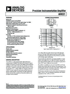
www.analog.comPrecision Instrumentation Amplifier AD8221 Rev. C Information furnished by Analog Devices is believed to be accurate and reliable. However, no responsibility is assumed by Analog Devices for its use, nor for any infringements of patents or other …

OPA657 1.6-GHz, Low-Noise, FET-Input Operational Amplifier ...
www.ti.comAmplifier Wideband Photodiode Transimpedance Amplifier 1 An IMPORTANT NOTICE at the end of this data sheet addresses availability, warranty, changes, use in safety-critical applications, intellectual property matters and other important disclaimers. PRODUCTION DATA.
Low Noise Amplifier, 0.01 GHz to 10 GHz Data Sheet ...
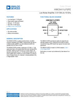
www.analog.comelectron mobility transistor (pHEMT), low noise wideband amplifier that operates from 0.01 GHz to 10 GHz. The HMC8411LP2FE provides a typical gain of 15.5 dB, a 1.7 dB typical noise figure, and a typical output third-order intercept (OIP3) of 34 dBm, requiring only 55 mA from a 5 V supply voltage. The saturated output power (P SAT) of 19.5 dBm

Single Sideband Modulation (SSB)
www.ee.ryerson.caamplifier Tunable RF stage Demodulator • The above system will function as required. However, the design and implementation of a tunable front-end, the RF stage, with sharp cut-off frequencies and high gain over a wide-range of frequencies, is a difficult task. • Consider the following scenarios 47 fc1 fc2 fc3 fc1 fc2 fc3 Signal mixed