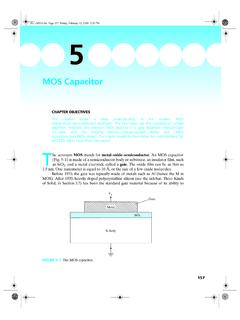
MOS Capacitor - Chenming Hu
advanced transistors (see Section 7.4). The MOS capacitor is not a widely used device in itself. However, it is part of the MOS transistor—the topic of the next tw o chapters. The MOS transistor is by far the most widely used semiconductor device. An MOS transistor (Fig. 5–2) is an MOS capacitor with two PN junctions flanking the capacitor.
Download MOS Capacitor - Chenming Hu

Information
Domain:
Source:
Link to this page:
Documents from same domain
MOS Transistor - Chenming Hu
www.chu.berkeley.eduModern MOSFET technology has advanced continually since its beginning in the 1950s. Figure 6–5 is a transmission electron microscope view of a part of a MOSFET. It shows the poly-Si gate and the single-crystalline Si body with visible individual Si atoms and a 1.2 nm amorphous SiO 2 film between them. 1.2 nm is the size of four SiO 2 molecules.

Device Fabrication Technology1 - Chenming Hu
www.chu.berkeley.edustarting material. A large wafer fab can process 40,000 silicon wafers into circuits each month. The simple example of the device fabrication process shown in Fig. 3–1 includes (a) formation of an SiO 2 layer, (b) its selective removal, (c) introduction of dopant atoms into the wafer surface, and (d) dopant diffusion into silicon. VLSI! ULSI!

Bipolar Transistor
www.chu.berkeley.eduIt was the first mass produced transistor, ahead of the MOS field-effect transistor (MOSFET) by a decade. After the introduction of metal-oxide-semiconductor (MOS) ICs around 1968, the high-density and low-power advantages of the MOS technology steadily eroded the BJT’s early dominance. BJTs are still pref erred in some high-frequency and analog

MOSFETs in ICs—Scaling, Leakage, and Other Topics
www.chu.berkeley.eduThe electron and hole mobility can be raised (or lowered) by carefully engineered mechanical strains. The strain changes the lattice constant of the silicon crystal and therefore the E–k relationship through the Schrodinger’s wave equation. The E–k relationship, in turn, determines the effective mass and the mobility.
Electrons and Holes in Semiconductors
www.chu.berkeley.eduevery silicon atom has four other silicon atoms as its nearest neighbor atoms. This fact is illustrated in Fig. 1–2 with the darkened cluster of a center atom having four neighboring atoms. This cluster is called the primitive cell. Silicon is a group IV element in the periodic table and has four valence electrons. These four electrons
PN and Metal–Semiconductor Junctions
www.chu.berkeley.edu4.1 Building Blocks of the PN Junction Theory 93 (4.1.2) The built-in potential is determined by N a and N d through Eq. (4.1.2). The larger the N a or N d is, the larger the φbi is.Typically, φbi is about 0.9 V for a silicon PN junction. Since a lower E c means a higher voltage (see Section 2.4), the N side is at a higher voltage or electrical potential than the P side.
Motion and Recombination of Electrons and Holes
www.chu.berkeley.educollisions is typically 10–13s or 0.1 ps (picosecond), and the distance between collisions is a few tens of nanometers or a few hundred angstroms. The net thermal velocity (averaged over time or over a large number of carriers at any given time) is zero. Thus, thermal motion does not create a steady electric current, but it does introduce a
Related documents
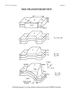
MOS TRANSISTOR REVIEW
web.stanford.eduMOS Device Scaling Na P N+ N+ L xox Xj o l P N+ S G D Scaled MOS Transistor Why do we scale MOS transistors? 1. Increase device packing density 2. Improve frequency response (transit time) α 1 L 3. Improve current drive (transconductance gm) g I V V const W L K t V V linear region W L K t V V V saturation region m D G D n ox ox DD n ox ox GT D ...

Lecture 15: MOS Transistor models: Body effects, SPICE models
inst.eecs.berkeley.edumodes of operation of a MOS FET: – Voltage controlled resistor model – I-V curve (Square-Law Model) – Saturation model In this lecture, we will: – add a correction due to the changing depletion region, called the body effect – Produce small signal models for the FET – and look at how MOS Transistors are modeled in SPICE
Lecture 24 MOSFET Basics (Understanding with no math ...
alan.ece.gatech.edun-channel MOS Transistor G=Gate, D=Drain, S=Source, B=Body (substrate, but to avoid confusion with substrate, B is used) G S D B V SG V SB V SD---+ p-channel MOS Transistor Note: All voltages are shown in their “positive “ direction. Obviously, V YX =-V XY for any voltage MOS Transistor Qualitative Description

8. MOS Transistors, CMOS Logic Circuits
web.stanford.eduMOS Transistors, CMOS Logic Circuits, and Cheap, Powerful Computers. M. Horowitz, J. Plummer, R. Howe 2 Reading • Chapter 4 in the reader • For more details look at –A&L 5.1 Digital Signals (goes in much more detail than we need) –A&L 6-6.3 MOS Devices. M. Horowitz, J. Plummer, R. Howe 3
MOS Transistor - Chenming Hu
www.chu.berkeley.eduMOS Transistor CHAPTER OBJECTIVES This chapter provides a comprehensive introduction to the modern MOSFETs in their on state. (The off state theory is the subject of the next chapter.) It covers the topics of surface mobility, body effect, a simple IV theory, and a more complete theory applicable to both long- and short-channel MOSFETs.

3. Short Channel Effects on MOS Transistors.
csit-sun.pub.rovariations in MOS transistors and mismatches in the emitter areas of bipolar devices. 3: Short Channel Effects 19 Institute of Microelectronic Systems Impact of Device Variations. 1.10 1.20 1.30 1.40 1.50 1.60 Leff (in mm) 1.50 1.70 1.90 2.10 Dela y …

MOS Transistor Theory
people.ee.duke.eduMOS Transistor Theory • So far, we have viewed a MOS transistor as an ideal switch (digital operation) – Reality: less than ideal. EE 261 James Morizio 2. EE 261 James Morizio 3 Introduction • So far, we have treated transistors as ideal switches • An ON transistor passes a finite amount of current – Depends on terminal voltages ...
Dynamic Combinational Circuits
people.ee.duke.edu– Transistors are leaky (I OFF „ 0) – Dynamic value will leak away over time – Formerly miliseconds, now nanoseconds! • Use keeper to hold dynamic node – Must be weak enough not to fight evaluation A f H 2 2 1 k X Y weak keeper. James Morizio 15 Charge Sharing (redistribution) Mp M e VDD Out A

5 MOS Field-Effect Transistors (MOSFETs)
learninglink.oup.com5 MOS Field-Effect Transistors (MOSFETs) Section 5.1: Device Structure and Physical Operation 5.1 An NMOS transistor is fabricated in a 0.13-µm CMOS process with L = 1.5Lmin and W = 1.3 µm. The process technology is specified to have tox =2.7nm, μn =400cm2/V·s, and Vtn =0.4V. (a) Find Cox, kn,andkn. (b) Find the overdrive voltage VOV and ...