
Phase Locked Loop Circuits
A PLL is a feedback system that includes a VCO, phase detector, and low pass filter within its loop. Its purpose is to force the VCO to replicate and track the frequency and phase at the input when in lock. The PLL is a control system allowing one oscillator to track with another. It is possible to have a phase offset between input and
Download Phase Locked Loop Circuits

Information
Domain:
Source:
Link to this page:
Documents from same domain

Transistor Technologies for High Efficiency and Linearity
web.ece.ucsb.eduDifferential Topology • Double the available voltage swing • Even-order harmonic suppression • Double the frequency of current injection into substrate –Reduce the potential for LO-pulling • The tail current source is removed from the standard differential pair (this is a “quasi-differential” structure) –DC current set by the biasing of input devices

ADS Tutorial Stability and Gain Circles ECE145A/218A
web.ece.ucsb.eduequations. The syntax is: gp_circle(S, gain, # points on circle) where S is the S-parameter matrix. Let’s illustrate. In the example below, a table is used to display frequency, maximum stable gain (MSG), the stability factor, k, and the magnitude of delta. The gain circles are at MSG (MaxGain1 in this case), and 1 and 2 dB below MSG.
Audio Amplifier Circuit - UC Santa Barbara
web.ece.ucsb.eduWeek #1: Audio amplifier Week #2: Microphone circuit The audio amplifier project is more difficult and time-consuming than the microphone pre-amp, so part of week #2 may be used to finish the audio amp. All breadboarding and testing can and should be done in lab. Soldering and hardwiring can and should be done outside lab.

Harmonic Balance Simulation on ADS
web.ece.ucsb.eduHarmonic Balance Simulation on ADS General Description of Harmonic Balance in Agilent ADS 1 Harmonic balance is a frequency-domain analysis technique for simulating nonlinear circuits and systems. It is well-suited for simulating analog RF and microwave circuits, ... function is driven to a given small value), then the resulting voltage ...
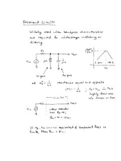
Quality factor, Q
web.ece.ucsb.eduWhen a resonant circuit is connected to the outside world, its total losses (let’s call them RP or GP) are combined with the source and load resistances, RS and RL. For example, Here is a parallel resonant circuit (C,L and RP)connected to the outside. The total Q of this circuit is called the loaded Q or QL and is given by

Latches, the D Flip-Flop & Counter Design
web.ece.ucsb.eduFebruary 6, 2012 ECE 152A - Digital Design Principles 2 Reading Assignment Brown and Vranesic 7Flip-Flops, Registers, Counters and a Simple Processor 7.1 Basic Latch 7.2 Gated SR Latch 7.2.1 Gated SR Latch with NAND Gates 7.3 Gated D …

Flip-Flops and Sequential Circuit Design
web.ece.ucsb.edu11 Latches and Flip-Flops 11.5 S-R Flip-Flop 11.6 J-K Flip-Flop 11.7 T Flip-Flop 11.8 Flip-Flops with Additional Inputs 11.9 Summary 12 Registers and Counters 12.5 Counter Design Using S-R and J-K Flip-Flops 12.6 Derivation of Flip-Flop Input Equations – Summary

BASICS OF THE SPECTRUM ANALYZER - UC Santa Barbara
web.ece.ucsb.eduFourier ⋅ π → − + + Now instead of a bank of narrow filters, we shall have one narrow filter centered at a fixed frequency, say fI, and we shall scan the signal spectrum across this filter by multiplying x(t) by a sinusoid of varying frequency f0. See Figure 1. …

Mealy and Moore Machines
web.ece.ucsb.eduFebruary 22, 2012 ECE 152A - Digital Design Principles 5 Finite State Machines Two types (or models) of sequential circuits (or finite state machines) Mealy machine Output is function of present state and present input Moore machine Output is function of present state only Analysis first, then proceed to the design of
Number Representation and Computer Arithmetic
web.ece.ucsb.eduOne way to encode decimal digits using binary signals is to encode each of the digits 0-9 by means of its 4-bit binary representation. The resulting binary-coded decimal (BCD) representation is shown below:
Related documents

Introduction to Switched-Capacitor Circuits
www.seas.ucla.educontrol the operation: S1 and 3 connect the left plate of C 1 to V in and ground, respectively, and Vout Vin C C1 2 S3 S1 S2 Figure 12.4. Switched-capacitor amplifier. S 2 provides unity-gain feedback. We first assume the open-loop gain of the op amp is very large and study the circuit in two phases. First, S1 and 2 are on and 3 is off ...
CIRCUITS LABORATORY EXPERIMENT 9 Operational Amplifiers
classes.engineering.wustl.eduthe phase relationship, peak-to-peak voltages and period. Now, measure the rms values of the input and output voltages. Compare your measurements to those predicted by Equation (9.2) above. Repeat the above exercise for Rf = 0 Ohms, i.e., a short circuit. Next, choose values for Ri and Rf such that the closed-loop gain (Vo / Vi) is 2.

TL494 - Switch mode Pulse Width Modulation Control Circuit
www.onsemi.comModulation Control Circuit TL494, NCV494 The TL494 is a fixed frequency, pulse width modulation control ... Open Loop Voltage Gain ( VO = 3.0 V, VO = 0.5 V to 3.5 V, RL = 2.0 k ) AVOL 70 95 − dB ... Standby Supply Current (Pin 6 at Vref, All other inputs and outputs open) (VCC = 15 V) (VCC = 40 V) ICC

CD4046B Phase-Locked Loop: A Versatile Building Block for ...
www.ti.comCD4046B Phase-Locked Loop: A Versatile Building ... stages, control gating, and a 3-state output circuit comprising p and n drivers having a common output node (see Figure 3). ... and the phase-comparator output becomes an open circuit and holds the voltage on the capacitor of the LPF constant. Moreover, the signal at the phase-pulses
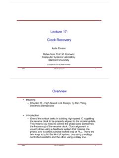
Lecture 17: Clock Recovery - Stanford University
web.stanford.edu• The basic circuit block is a Phase Locked Loop Tx RxChannel T-clk R-clk MAH EE 371 Lecture 17 4 ... phase margin Open-loop TF ω z 1 40dB/decade Closed-loop TF K pd *K f*K vco Mag 1 T(s) H(s) peaking i.e: we are adding proportional control (z 1) to adjust the output phase while the ¼ lter integrator (pole at 1/s) holds the frequency ...
9.0 GENERATOR, EXCITER, AND VOLTAGE REGULATION
www.nrc.govbetween the open ends of the ‘U’. A coil of wire is wrapped about the legs of this form to produce a magnetic field across the gap. In the gap, an armature is formed by a loop of wire. The loop exits the armature onto two slip rings. The slip rings are contacted by brushes that connect the generator to the outside electric circuit. An engine or
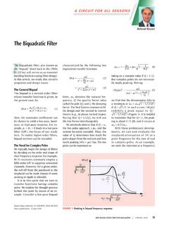
The Biquadratic Filter - University of California, Los Angeles
www.seas.ucla.eduzero to the open-loop transfer func-tion, as practiced in type II phase-locked loops, or 2) we can make one of the integrators lossy, e.g., we can change ks 1/ to ks 1/( +a). The latter is realized if a fraction of the integrator’s output is returned to its input without phase shift. Illustrated in Figure 3(a), such an arrangement yields . A ...

Open Quantum Assembly Language
arxiv.orgThe remaining sections of this document specify Open QASM and provide examples. 2 Language The syntax of the human-readable form of Open QASM has elements of C and assembly languages. The rst (non-comment) line of an Open QASM program must be OPENQASM M.m; indicating a major version M and minor version m. Version 2.0 is described in this document.
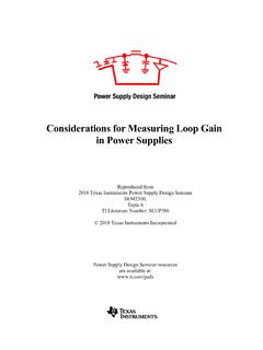
Considerations for Measuring Loop Gain in Power Supplies
www.ti.comFigure 6 – Measuring loop gain of a power supply in open-loop setup. When the feedback loop is broken at any point, such as that shown in Figure 6, looking backward, i.e. looking into point B, and applying Thevenin’s theory, the circuit is equivalent to a voltage-controlled voltage source (VCVS) in series with an output impedance, Z