
Power Semiconductor Reliability Handbook
Power Semiconductor Reliability Handbook ... There are certain wear-out mechanisms in a semiconductor device, such as electromigration, hot carrier degradation of a ... time, if the design rules given by a reputable silicon foundry are …
Download Power Semiconductor Reliability Handbook

Information
Domain:
Source:
Link to this page:
Documents from same domain

AOD4185/AOI4185 P-Channel Enhancement Mode …
www.aosmd.comParameter Symbol Maximum Units Absolute Maximum Ratings T C=25°C unless otherwise noted AOD4185/AOI4185 P-Channel Enhancement Mode Field Effect Transistor Features VDS (V) = -40V

High Voltage Power MOSFET switching …
www.aosmd.comHigh Voltage Power MOSFET switching parameters: Testing Methods for Guaranteeing datasheet limits Anup Bhalla, Fei Wang Introduction Power MOSFET datasheets will usually show typical and min-max values for Rg, Ciss, Crss, Coss, and also show values

Alpha and Omega Semiconductor Corporate …
www.aosmd.comAOS Corporate Responsibility 2 14064-1 worldwide standard, which means that we d evelop and implement programs to limit greenhouse gas (GHG) concentrations.

Continous Drain current rating and Bonding wire …
www.aosmd.comPower MOSFET Continuous Drain current rating and Bonding wire limitation Fei Wang , Kai Liu, Anup Bhalla Abstract Power MOSFET datasheets will usually show maximum values for continuous drain current Id, on the first page of

Power MOSFET Basics - Alpha and Omega …
www.aosmd.com1 Power MOSFET Basics Table of Contents 1. Basic Device Structure 2. Breakdown Voltage 3. On-State Characteristics 4. Capacitance 5. Gate Charge

100V N-Channel MOSFET
www.aosmd.comAOD478/AOI478 TYPICAL ELECTRICAL AND THERMAL CHARACTERISTICS 17 5 2 10 0 18 0 2 4 6 8 10 0 2 4 6 8 10 12 V GS (Volts) Qg …

Alpha & Omega Semiconductor
www.aosmd.com4 Summary of AOS Device / Process Qualification Monitor Results To present the actual FIT rate from the different process and device technologies, AOS

General Description Product Summary
www.aosmd.comAOD409/AOI409 TYPICAL ELECTRICAL AND THERMAL CHARACTERISTICS 0 2 4 6 8 10 0 10 20 30 40 50 60-V GS s) Q g (nC) Figure 7: Gate-Charge Characteristics 500

General Description Product Summary - Alpha and …
www.aosmd.comAO4294 General Description Product Summary VDS I D (at V GS =10V) 11.5A R DS(ON) (at V GS =10V) < 12mΩ R DS(ON) (at V GS =4.5V) < 15.5mΩ Applications 100% UIS Tested 100% Rg Tested Symbol

General Description Product Summary - Alpha and …
www.aosmd.comaonr21357 typical electrical and thermal characteristics 0 100 200 300) 400 500 1e-05 0.0001 0.001 0.01 0.1 1 10 100 pulse width (s)
Related documents

SEMICONDUCTOR DEVICE PHYSICS AND DESIGN
seklad69associates.comSemiconductor Device Physics and Design UMESH K. MISHRA University of California, Santa Barbara, CA, USA and JASPRIT SINGH The University of Michigan, Ann Arbor, MI, USA
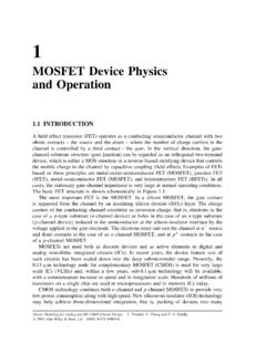
MOSFET Device Physics and Operation
homepages.rpi.educase of a p-type substrate (n-channel device) or holes in the case of an n-type substrate (p-channel device), induced in the semiconductor at the silicon-insulator interface by the voltage applied to the gate electrode. The electrons enter and exit the channel at n+ source and drain contacts in the case of an n-channel MOSFET, and at p+ ...
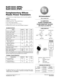
Complementary Silicon Plastic Power ... - ON Semiconductor
www.onsemi.comTotal Power Dissipation @ TA = 25 C Derate above 25 C PD 2.0 0.016 W W/ C Operating and Storage Junction Temperature Range TJ, Tstg –65 to +150 C ESD − Human Body Model HBM 3B V ESD − Machine Model MM C V Stresses exceeding those listed in the Maximum Ratings table may damage the device. If any of these limits are exceeded, device ...
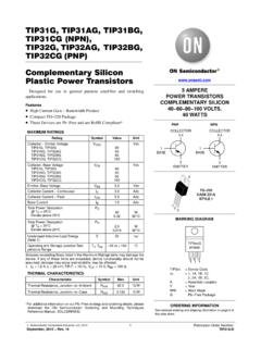
Complementary Silicon Plastic Power ... - ON Semiconductor
www.onsemi.comTotal Power Dissipation @ TA = 25°C Derate above 25°C PD 2.0 0.016 W W/°C Unclamped Inductive Load Energy (Note 1) E 32 mJ Operating and Storage Junction Tem-perature Range TJ, Tstg –65 to +150 °C Stresses exceeding those listed in the Maximum Ratings table may damage the device. If any of these limits are exceeded, device functionality ...

Lecture 2. Power semiconductor devices (Power switches)
www.philadelphia.edu.jopower supplies. 2.2 Thyristors ( Silicon Controlled Rectifiers “SCRs”) The thyristor ,it is also called silicon controlled rectifier (SCR), is a four-layer, three terminal switching semiconductor device, with each layer consisting of an alternately N or P-type material, for example N-P-N-P. The main terminals,
Gallium Nitride (GaN) versus Silicon Carbide (SiC)
www.richardsonrfpd.comapplications are Gallium Nitride (GaN) and Silicon Carbide (SiC). There is a great deal of on-going discussion and questions about Gallium Nitride (GaN) versus Silicon Carbide (SiC) material, the semiconductor devices which are possible and which device / material is best suited for various switching and RF power applications.

Introduction to Semiconductor Technology ...
www.st.comINTRODUCTION TO SEMICONDUCTOR TECHNOLOGY by Microcontroller Division Applications INTRODUCTION An integrated circuit is a small but sophisticated device implementing several electronic func-tions. It is made up of two major parts: a tiny and very fragile silicon chip (die) and a package

Wide Bandgap Semiconductors: Pursuing the Promise
www1.eere.energy.govWide bandgap (WBG) semiconductor . materials allow power electronic components to be smaller, faster, more reliable, and more efficient than their silicon (Si)-based counterparts. These capabilities make it possible to reduce weight, volume, and life-cycle costs in a wide range of power applications. Harnessing these capabilities can lead