
SEMICONDUCTOR MEMORIES
The read-out of the 1T DRAM cell is destructive; read and refresh operations are necessary for correct operation. Unlike 3T cell, 1T cell requires presence of an extra capacitance that must be explicitly included in the design. When writing a “1” into a DRAM cell, a threshold voltage is lost.
Download SEMICONDUCTOR MEMORIES

Information
Domain:
Source:
Link to this page:
Documents from same domain

chapter2.fm Page 33 Monday, September 4, 2000 …
bwrcs.eecs.berkeley.eduIC packaging Future Trends in Integrated Circuit Technology 2.1 Introduction 2.2 Manufacturing CMOS Integrated Circuits 2.2.1 The Silicon Wafer 2.2.2 Photolithography 2.2.3 Some Recurring Process Steps ... cess that lies at the core of the semiconductor revolution. Yet, some insight in the steps ...

Designing a Divider - University of California, Berkeley
bwrcs.eecs.berkeley.eduDigital Integrated Circuits 2/e DIVIDE HARDWARE Version 1 ° 64-bit Divisor reg, 64-bit ALU, 64-bit Remainder reg, 32-bit Quotient reg Remainder Quotient Divisor …
CMOS Manufacturing Process
bwrcs.eecs.berkeley.eduDigital Integrated Circuits Manufacturing Process EE141 A Modern CMOS Process p-well n-well p+ p-epi SiO 2 AlCu poly n+ SiO 2 p+ gate-oxide Tungsten TiSi 2 Dual-Well Trench-Isolated CMOS Process
Lecture 9: Digital Signal Processors: Applications and ...
bwrcs.eecs.berkeley.eduProcessor Applications General Purpose - high performance ... Digital camera - TMS320C5000 ... DSP evolved from Analog Signal Processors, using analog hardware to transform phyical signals (classical electrical engineering) ASP to DSP because

DESIGNING COMBINATIONAL LOGIC GATES IN CMOS
bwrcs.eecs.berkeley.edu198 DESIGNING COMBINATIONAL LOGIC GATES IN CMOS Chapter 6 6.1Introduction The design considerations for a simple inverter circuit ere presented in the previousw chapter. In this chapter, the design of the inverter will be extended to address the synthesis

DESIGNING SEQUENTIAL LOGIC CIRCUITS
bwrcs.eecs.berkeley.edu272 DESIGNING SEQUENTIAL LOGIC CIRCUITS Chapter 7 7.1 Introduction Combinational logic circuits that were described earlier have the property that the output

Lecture11-MOS Cap Delay
bwrcs.eecs.berkeley.eduEE141 25 EECS141 Lecture #11 25 The Miller Effect V in M1 C gd1 V out ∆V As V in increases, V out drops – Once get into the transition region, gain from V in to V out > 1 So, C gd experiences voltage swing larger than V
Chapter 4 Calculating the Logical Effort of Gates
bwrcs.eecs.berkeley.edu4.3 Calculating logical effort Definition 4.2 provides a convenient method for calculating the logical effort of a logic gate. We have but to design a gate that has the same current drive character-istics as a reference inverter, calculate the input capacitances of each signal, and apply Equation 4.1 to obtain the logical effort.

DESIGNING COMBINATIONAL LOGIC GATES IN CMOS
bwrcs.eecs.berkeley.eduof arbitrary digital gates such as NOR, NAND and XOR. The focus will be on combina-tional logic (or non-regenerative) circuits that have the property that at any point in time, the output of the circuit is related to its current input signals by some Boolean expression (assuming that the transients through the logic gates have settled).

Introduction to OFDM
bwrcs.eecs.berkeley.eduOFDM Introduction EE225C Introduction to OFDM lBasic idea ... – Selective Fading – Very short pulses – ISI iscompartively long – EQs are then very long – Poor spectral efficiency because of band guards Drawbacks ... 2 4 6 8 10 12 14 16-60-55-50-45-40-35-30-25-20-15-10
Related documents

NAND vs. NOR Flash Memory Technology Overview
aturing.umcs.maine.eduApr 25, 2006 · Toshiba NAND vs. NOR Flash Memory Technology Overview Page 3 NOR vs. NAND Flash Density For any given lithography process, the density of the NAND Flash memory array will always be higher than NOR Flash. In theory, the highest density NAND will be at least twice the density of NOR, for the same process technology and chip size.

Samsung PM1725b NVMe SSD
image-us.samsung.com3D vertical-NAND (V-NAND) flash memory and an optimized controller. • Outstanding reliability Features three DWPD (drive writes per day) for five years, which equates to 38.4TBs daily, or 7,680 files of 5GB-equivalent data or video every day. • High capacities The 1725b supports a range of capacities, from 1.6TB to an industry leading 15.36TB.
WD Blue 3D NAND SATA SSD - Western Digital
documents.westerndigital.comVolatile cache — DDR DRAM cache Tiered Caching structure — A non-volatile flash write cache Mass storage — TLC NAND flash The tiered caching structure is a pool of X1 blocks which are used as write cache to accumulate and consolidate all writes at …

Porting U-Boot and Linux on new ARM boards: a step-by-step ...
elinux.orgGolden rules If you have the sources of your BSP, compile and run the BSP to: 1. Validate the IP you’re working on works with some code, 2. Have a reference code, 3. Have a code that you can use to debug, Focus on correctly configuring RAM and UART only, Commit, One IP at a time, Commit, FreeElectrons- Embedded Linux, kernel, drivers - Development, consulting, training …

Data Sheet SAMSUNG PROPRIETARY Samsung V-NAND SSD …
www.samsung.comNAND Flash Memory Samsung V-NAND 3bit MLC DRAM Cache Memory 1GB LPDDR4 2GB LPDDR4 Dimension Max 80.15 x Max 24.15 x Max 8.6 (mm) Form Factor M.2 (2280) Performance (Up to.)2) 3) 4) Sequential Read 7,000 MB/s 7,000 MB/s Sequential Write 5,000 MB/s 5,100 MB/s QD 1 Thread 1 Ran. Read 22K IOPS Ran. Write 60K IOPS 60K IOPS QD 32 …
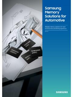
Samsung Memory Solutions for Automotive
www.samsung.comautomotive Flash Memory delivers high reliability, extensive product and technical support to keep pace with the long auto production life cycle and a broad portfolio for enhanced customization and compatibility. Samsung's advanced memory solutions for automotive applications NAND Flash Solutions (UFS / eMMC) • Meet AEC-Q100

DM SM2263EN SM2263XT vNF - Silicon Motion
www.siliconmotion.comNAND Flash Channel CE/Channel Max Performance DRAM Interface NAND Flash Support Security Temperature Support Package PCIe Gen3 x4 NVMe 1.3 4 4 Sequential Read: 2,400 MB/s Sequential Write: 1,700 MB/s Random Write: 250K IOPS Supports DDR3, DDR3L, LPDDR3 and DDR4 16-bit data bus width 2 chip enable pins PCIe Gen3 x4 NVMe 1.3 4 4 Sequential …