
SEMICONDUCTOR MEMORIES
Semiconductor Memory Classification RWM NVRWM ROM EPROM E2PROM FLASH Random Access Non-Random Access SRAM DRAM Mask-Programmed Programmable (PROM) FIFO Shift Register CAM ... Metal bypass K cells Polysilicon word line WL Polysilicon word line Driver (b) Using a metal bypass (a) Driving the word line from both sides Metal word line WL
Download SEMICONDUCTOR MEMORIES

Information
Domain:
Source:
Link to this page:
Documents from same domain
chapter2.fm Page 33 Monday, September 4, 2000 …
bwrcs.eecs.berkeley.eduIC packaging Future Trends in Integrated Circuit Technology 2.1 Introduction 2.2 Manufacturing CMOS Integrated Circuits 2.2.1 The Silicon Wafer 2.2.2 Photolithography 2.2.3 Some Recurring Process Steps ... cess that lies at the core of the semiconductor revolution. Yet, some insight in the steps ...

Designing a Divider - University of California, Berkeley
bwrcs.eecs.berkeley.eduDigital Integrated Circuits 2/e DIVIDE HARDWARE Version 1 ° 64-bit Divisor reg, 64-bit ALU, 64-bit Remainder reg, 32-bit Quotient reg Remainder Quotient Divisor …
CMOS Manufacturing Process
bwrcs.eecs.berkeley.eduDigital Integrated Circuits Manufacturing Process EE141 A Modern CMOS Process p-well n-well p+ p-epi SiO 2 AlCu poly n+ SiO 2 p+ gate-oxide Tungsten TiSi 2 Dual-Well Trench-Isolated CMOS Process
Lecture 9: Digital Signal Processors: Applications and ...
bwrcs.eecs.berkeley.eduProcessor Applications General Purpose - high performance ... Digital camera - TMS320C5000 ... DSP evolved from Analog Signal Processors, using analog hardware to transform phyical signals (classical electrical engineering) ASP to DSP because

DESIGNING COMBINATIONAL LOGIC GATES IN CMOS
bwrcs.eecs.berkeley.edu198 DESIGNING COMBINATIONAL LOGIC GATES IN CMOS Chapter 6 6.1Introduction The design considerations for a simple inverter circuit ere presented in the previousw chapter. In this chapter, the design of the inverter will be extended to address the synthesis

DESIGNING SEQUENTIAL LOGIC CIRCUITS
bwrcs.eecs.berkeley.edu272 DESIGNING SEQUENTIAL LOGIC CIRCUITS Chapter 7 7.1 Introduction Combinational logic circuits that were described earlier have the property that the output

Lecture11-MOS Cap Delay
bwrcs.eecs.berkeley.eduEE141 25 EECS141 Lecture #11 25 The Miller Effect V in M1 C gd1 V out ∆V As V in increases, V out drops – Once get into the transition region, gain from V in to V out > 1 So, C gd experiences voltage swing larger than V
Chapter 4 Calculating the Logical Effort of Gates
bwrcs.eecs.berkeley.edu4.3 Calculating logical effort Definition 4.2 provides a convenient method for calculating the logical effort of a logic gate. We have but to design a gate that has the same current drive character-istics as a reference inverter, calculate the input capacitances of each signal, and apply Equation 4.1 to obtain the logical effort.

DESIGNING COMBINATIONAL LOGIC GATES IN CMOS
bwrcs.eecs.berkeley.eduof arbitrary digital gates such as NOR, NAND and XOR. The focus will be on combina-tional logic (or non-regenerative) circuits that have the property that at any point in time, the output of the circuit is related to its current input signals by some Boolean expression (assuming that the transients through the logic gates have settled).
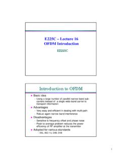
Introduction to OFDM
bwrcs.eecs.berkeley.eduOFDM Introduction EE225C Introduction to OFDM lBasic idea ... – Selective Fading – Very short pulses – ISI iscompartively long – EQs are then very long – Poor spectral efficiency because of band guards Drawbacks ... 2 4 6 8 10 12 14 16-60-55-50-45-40-35-30-25-20-15-10
Related documents
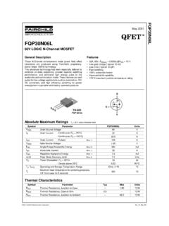
FQP30N06L 60V LOGIC N-Channel MOSFET
cdn.sparkfun.com©2001 Fairchild Semiconductor Corporation Rev. A1. May 2001 0 5 10 15 20 25 30 0 2 4 6 8 10 12 V DS = 30V V DS = 48V ※ Note : I D = 32A V GS, Gate-Source Voltage [V] Q G, Total Gate Charge [nC] 10-1 100 101 0 500 1000 1500 2000 C iss = C gs + C gd (C ds = shorted) C oss = C ds + C gd C rss = C gd ※ Notes : 1. V GS = 0 V 2. f = 1 MHz C rss ...

Chapter 9 Metal-Semiconductor Contacts
inst.eecs.berkeley.eduSemiconductor Devices for Integrated Circuits (C. Hu) Slide 9-6 Schottky barrier heights of metal silicide on Si Silicide-Si interfaces are more stable than metal-silicon interfaces. After metal is deposited on Si, an annealing step is applied to form a silicide-Si contact. The term metal-silicon contact includes silicide-Si contacts.

Metal/Semiconductor Ohmic Contacts - Stanford University
web.stanford.eduis a constant dependent upon metal and the semiconductor. Specific contact resistivity, ρ c primarily depends upon • the metal-semiconductor work function, φΒ, • doping density, N, in the semiconductor and • the effective mass of the carrier, m*.

AppCompendium Semiconductor ICP-MS-5991-9495EN-US …
www.agilent.comMay 01, 2012 · Agilent ICP-MS Solutions for the Semiconductor Industry 8 Automating Analysis of Metal Contaminants in Si Wafers 9 Setups for Different Sample Types 11 Expanding Capabilities with Accessories and Software 15 Online Monitoring of Metal Contaminants in Process Chemicals 16 Contamination Control 17 ICP-MS Applications 18 Cleaning/Etching 19

Marking Transition Brochure ON Semiconductor Part
www.electro-tech-online.comOn August 5th, 1999 Motorola's former Semiconductor Components Group emerged as ON Semiconductor, an independent company focused on standard discrete, logic and analog semiconductor products. As part of the terms of separation ON Semiconductor was granted the ability to manufacture and sell Motorola logo-marked products for one year.

Introduction to Semiconductor Technology ...
www.st.comINTRODUCTION TO SEMICONDUCTOR TECHNOLOGY 2 BASIC IC ELEMENT: THE TRANSISTOR 2.1 MOS TECHNOLOGY We will examine first the basics of MOS (Metal Oxide Semiconductor) technologies as they are used for the majority of the integrated circuits manufactured at STMicroelectronics.

Metal Can Packages (TO-3/5/8/18/39/46/52/72)
www.ti.comNational Semiconductor Corporation Americas Tel: 1-800-272-9959 Fax: 1-800-737-7018 Email: support@nsc.com National Semiconductor Europe Fax: +49 (0) 1 80-530 85 86 Email: europe.support@nsc.com Deutsch Tel: +49 (0) 1 80-530 85 85 English Tel: +49 (0) 1 80-532 78 32 Français Tel: +49 (0) 1 80-532 93 58 Italiano Tel: +49 (0) 1 80-534 16 80 ...