
TDA8932B Class-D audio amplifier
HVP2 19 half supply output voltage 2 for charging single-ended capacitor for channel 2 VDDP2 20 positive power supply voltage for channel 2 BOOT2 21 bootstrap high-side driver channel 2 OUT2 22 PWM output channel 2 VSSP2 23 negative power supply voltage for channel 2 STAB2 24 decoupling of internal 11 V regulator for channel 2 drivers
Download TDA8932B Class-D audio amplifier

Information
Domain:
Source:
Link to this page:
Documents from same domain

AN10441 Level shifting techniques in I2C-bus design
www.nxp.comDocument information AN10441 Level shifting techniques in I2C-bus design Rev. 01 — 18 June 2007 Application note Info Content Keywords I2C-bus, level shifting Abstract Logic level shifting may be required when interfacing legacy devices with

AN3234: Washing Machine Three-Phase AC …
www.nxp.comWashing Machine Three-Phase AC Induction Motor Drive, Rev. 0 Indirect Vector Control 4 Freescale Semiconductor If you are looking for more theory on the field ...

1. General description - nxp.com
www.nxp.com1. General description The TJA1044 is part of the Mantis family of high-speed CAN transceivers. It provides an interface between a Controller Area Network (CAN) protocol controller and the physical

PCA9570 Remote 4-bit general purpose outputs for 1 MHz …
www.nxp.com1. General description The PCA9570 is a CMOS device that provides 4 bits of General Purpose parallel Output (GPO) expansion in low voltage processor and handheld battery powered mobile

P82B96 Dual bidirectional bus buffer - nxp.com
www.nxp.com1. General description The P82B96 is a bipolar IC that creates a non-latching, bidirectional, logic interface between the normal I2C-bus and a range of other bus configurations.It can interface

S32K144 EVB Quick Start Guide - NXP Semiconductors
www.nxp.comJ14 SWD connector. 3 EXTERNAL USE S32K144 EVBFeatures: ... USB connector of the USB cable to micro-B port J7 on the S32K144EVB. ... Windows, Linux and Mac operating systems. Using the MSD Flash Programmer 1. Locate the .srec file of your project , file is under the

Three-Phase BLDC Motor Sensorless Control Using …
www.nxp.comThis document describes the design of a three-phase brushless DC motor (BLDC motor) drive based on Freescale’s MC56F8013 and MC56F8023 dedicated motor control device. Brushless DC motors are popular in a wide application area.

AN11443 BFU550XR ISM 433 MHz LNA design - nxp.com
www.nxp.comAN11443 BFU550XR ISM 433 MHz LNA design Rev. 1 — 23 January 2014 Application note . Document information Info Content Keywords BFU520, BFU530, BFU550 series, ISM-band, 433MHz 866MHz Abstract This document describes an ISM Frequency LNA design on BFU5xxXR Starter kit

DSP56156 16-Bit Digital Signal Processor - nxp.com
www.nxp.comThe DSP56156 is a general-purpose MPU-style Digital Signal Processor (DSP). On a single semi- conductor chip, the DSP56156 comprises a very efficient 16-bit digital signal processing core, pro-

SAA7706H Car radio Digital Signal Processor (DSP)
www.nxp.comCar radio Digital Signal Processor (DSP) SAA7706H This text is here in white to force landscape pages to be rotated correctly when browsing through the pdf in the Acrobat reader.This text is here in _white to force landscape pages to be rotated correctly when browsing through the pdf in the Acrobat reader.This text is here inThis text is here in
Related documents
Class D Amplifier Design Basics II - irf.com
www.irf.comdevices, such as finite ON resistance, finite switching speed or body diode characteristics. 5. Parasitic components that cause ringing on transient edges 6. Power supply voltage fluctuations due to its finite output impedance and reactive power flowing through the DC bus 7. Non-linearity in the output LPF. Note that 0.01% of non-linearity ...
Relay symbols and device numbers; selection from IEC 617 ...
library.e.abb.comfield, a machine armature, a capacitor, or a reactor. Note: This excludes devices that perform such shunting operations as may be necessary in the process of starting a machine by devices 6 or 42, or their equivalent, and also excludes device 73 function that serves for the switching of resistors. 18 Accelerating or decelerating
18-Bit - Multi-Channel Delta-Sigma Analog-to-Digital ...
ww1.microchip.comMar 26, 2009 · Technology Inc. These devices can convert analog inputs to digital codes with up to 18 bits of resolution. The on-board 2.048V reference voltage enables an input range of ± 2.048V differentially (full scale range = 4.096V/PGA). These devices can output analog-to-digital conversion results at rates of 3.75, 15, 60, or 240 samples per
6.5 V, 1 A, Ultralow Noise, High PSRR ... - Analog Devices
www.analog.com3 Current-limit threshold is defined as the current at which the output voltage drops to 90% of the specified typical value. For example, the current limit for a 5.0 V output voltage is defined as the current that causes the output voltage to drop to 90% of 5.0 V, or 4.5 V. INPUT AND OUTPUT CAPACITOR, RECOMMENDED SPECIFICATIONS Table 3.
6.5 V, 2 A, Ultralow Noise, High PSRR ... - Analog Devices
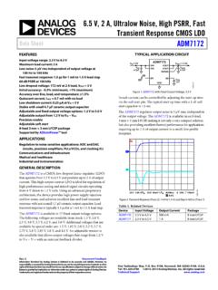
www.analog.comstart capacitor is 1.0 ms. The . ADM7172 regulator output noise is 5 μV rms, independent of the output voltage. The ADM7172 is available in an 8-lead, 3 mm × 3 mm LFCSP, making it not only a very compact solution, but also providing excellent thermal performance for applications requiring up to 2 A of output current in a small, low profile
Cadence Tutorial EN1600 - Brown University
www.brown.eduThe NCSU_Devices_FreePDK library provides four ... from which you can select the output node by clicking on the output net (wire). After the selection, the ... of the capacitor to the output node and the other terminal to gnd as in Figure 21. 12 ...

MMA7361L ±1.5g - 6g Three Axis Low-g Micromachined ...
www.nxp.com(recommended as a minimum to filter clock noi se) on the analog output for each axis and a 0.1 μF capacitor on V DD - GND. The output sensor bandwidth is determined by the Capacitor added on the output. f = 1/2π * (32 x 103) * C. C = 3.3 nF corresponds to BW = 1507HZ, which is the minimum to filter out internal clock noise. 2.
7 Series FPGAs and Zynq-7000 SoC XADC Dual 12-Bit 1 MSPS ...
www.xilinx.comCapacitor values were changed, a new 10 µF capacitor was added, and notes were added to Figure 6-1. Notes were added to Figure 6-5. XADC Software Support was completely replaced. In that section, the Verilog instantiation was replaced. Figure 6-6: Analog Stimulus File and Figure 6-7: XADC Simulation Output were deleted.