TUTORIAL - Analog Devices
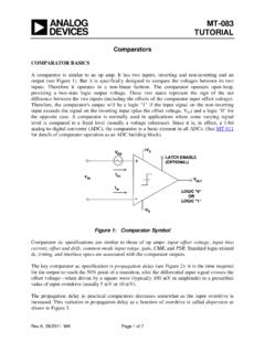
Rev.A, 09/2011, WK Page 1 of 7 MT-083 TUTORIAL Comparators . COMPARATOR BASICS . A comparator is similar to an op amp. It has two inputs, inverting and non-inverting and an output (see Figure 1). But it is specifically designed to compare the voltages between its two inputs. Therefore it operates in a non-linear fashion. The comparator operates ...
Download TUTORIAL - Analog Devices

Information
Domain:
Source:
Link to this page:
Documents from same domain

AD743 Ultralow Noise BiFET Op Amp Data Sheet …
www.analog.comREV. E Information furnished by Analog Devices is believed to be accurate and reliable. However, no responsibility is assumed by Analog Devices for its

MT-070: In-Amp Input RFI Protection - Analog …
www.analog.comRev.0, 10/08, WK Page 1 of 6 MT-070 TUTORIAL In-Amp Input RFI Protection . PROTECTING IN-AMPS AGAINST RFI . Real-world applications must deal with an ever increasing amount of radio frequency

LTC3108 - Ultralow Voltage Step-Up Converter and …
www.analog.comLTC3108 3108fc For more information www.linear.com/LTC3108 LDO

1.8 V Low Power CMOS Rail-to-Rail Input/Output …
www.analog.com1.8 V Low Power CMOS Rail-to-Rail Input/Output Operational Amplifier Data Sheet AD8515 Rev. E Document Feedback Information furnished by Analog Devices is believed to be accurate and reliable.

Low Cost Micropower, Low Noise CMOS Rail-to …
www.analog.comLow Cost Micropower, Low Noise CMOS Rail-to-Rail, Input/Output Operational Amplifiers Data Sheet AD8613/AD8617/AD8619 Rev. H Document Feedback Information furnished by Analog Devices is believed to be accurate and reliable.

Low Cost CMOS, High Speed, Rail-to-Rail Amplifiers
www.analog.comLow Cost CMOS, High Speed, Rail-to-Rail Amplifiers Data Sheet ADA4891-1/ADA4891-2/ADA4891-3/ADA4891-4 Rev. F Document Feedback Information furnished by Analog Devices ...

Zero-Drift, Single-Supply, Rail-to-Rail Input/Output ...
www.analog.comZero-Drift, Single-Supply, Rail-to-Rail Input/Output Operational Amplifier Data Sheet AD8628/AD8629/AD8630 FEATURES Lowest auto-zero amplifier noise Low offset voltage: 1 µV AD8628

FEATURES DESCRIPTIO U - analog.com
www.analog.com1 LT1025 1025fb DESCRIPTIO U APPLICATIO S U 80µA Supply Current 4V to 36V Operation 0.5°C Initial Accuracy (A Version) Compatible with Standard Thermocouples (E, J, K, R, S, T) Auxiliary 10mV/°C Output Available in 8-Lead PDIP and SO Packages Thermocouple Cold Junction Compensator Centigrade Thermometer Temperature …

LT1173 - Micropower DC/DC Converter Adjustable …
www.analog.comLT1173 1 Micropower DC/DC Converter Adjustable and Fixed 5V, 12V VOUT 5V/DIV 0V PROGRAM 5V/DIV 5ms/DIV 1173 TA02 L1* 100µH LT1173 • TA01 + GND SW2 FB SW1 ILIM VIN 10 F LT1173

AD9850 CMOS, 125 MHz Complete DDS …
www.analog.comrev. h a cmos, 125 mhz complete dds synthesizer ad9850 functional block diagram clock out clock out analog in analog out dac rset …
Related documents
Chapter 4 Low-Power VLSI DesignPower VLSI Design
www.ee.ncu.edu.tw4/4 1 0 t iti l k4/4 = 1.0 transition per clock • Gray-code counter is more power efficient.code counter is more power efficient. G. K. Yeap, Practical Low Power Digital VLSI Design, Boston: Kluwer Academic Publishers (now Springer) 1998 National Central University EE4012VLSI Design 30 Kluwer Academic Publishers (now Springer), 1998.

LM339 - Single Supply Quad Comparators
www.onsemi.comthe comparator will provide a proper output state. Refer to the Maximum Ratings table for safe operating area. ... CMOS TTL 1/4 MC14001 1/4 MC7400 +15 +5.0 100 10 RS = Source Resistance R1 RS T1 = T2 = 0.69 RC f 7.2 C( F) ... It is good design practice to ground all unused input pins. Differential input voltages may be larger than supply

Analog Integrated Circuit Design 2nd Edition
www.d.umn.edu10.1.1 Input offset and noise The input offset voltage of a comparator is the input voltage at which its output changes from one logic level to the other. It may be caused by device mismatch or may be inherent to the design of a comparator. Random circuit noise can cause the output to change from one logic level to the other, even
PIC12F629/675 Data Sheet
ww1.microchip.comAN1 AN A/D Channel 1 input CIN- AN Comparator input VREF AN External voltage reference ICSPCLK ST Serial programming clock GP2/AN2/T0CKI/INT/COUT GP2 ST CMOS Bi-directional I/O w/ programmable pull-up and interrupt-on-change AN2 AN A/D Channel 2 input T0CKI ST TMR0 clock input INT ST External interrupt COUT CMOS Comparator output GP3/MCLR/VPP

Examples of Solved Problems for Chapter3,5,6,7,and8
www.eecg.utoronto.caThen, X ≤ Y is detected by Z +(N ⊕V) = 1. The last two cases are just simple inverses: X>Yif Z +(N ⊕V)=1andX ≥ Y if N ⊕V =1. Figure 5.43. A comparator circuit. Example 6.25 Problem: Implement the function f(w1,w2,w3)= m(0,1,3,4,6,7) by …

2-Bit Magnitude Comparator Design Using Different Logic …
www.ijesi.org3. 2-BIT MAGNITUDE COMPARATOR DESIGN USING DIFFERENT LOGIC STYLES 3.1. Using CMOS Logic Style Fig.3 (a) represents symbol of CMOS Inverter. It consists of one NMOS & one PMOS transistor. If input A=0 (logic low) then both gates are at zero potential & PMOS is ON & provide low impedance path from V DD to output (Y).
LT1720/LT1721 - Dual/Quad, 4.5ns, Single Supply 3V/5V ...
www.analog.comLT1720/LT1721 3 17201fc ELECTRICAL CHARACTERISTICS SYMBOL PARAMETER CONDITIONS MIN TYP MAX UNITS VCC Supply Voltage l 2.7 6 V ICC Supply Current (Per Comparator) VCC = 5V VCC = 3V l l 4 3.5 7 6 mA mA VCMR Common Mode Voltage Range (Note 2) l –0.1 VCC – 1.2 V VTRIP+ Input Trip Points (Note 3) l –2.0 –3.0 5.5 6.5 mV mV …
CMOS Comparator Design
www.eecis.udel.eduVishal Saxena -1- CMOS Comparator Design Extra Slides Vishal Saxena, Boise State University (vishalsaxena@boisestate.edu) Vishal Saxena -2- Comparator Design Considerations

Design and Simulation of CMOS Schmitt Trigger
ijiset.comof Schmitt trigger is using CMOS technology in different foundry. Then, post-layout simulation of Schmitt trigger is done in Microwind 3.1 using90nm, 65nm and 45 nm CMOS technology. The design is implemented using DSCH software to calculate area and power consumption.