Transcription of Ultralow Noise, 200 mA, CMOS Linear Regulator Data Sheet ...
1 Data SheetADP151 Ultralow Noise, 200 mA, CMOS Linear RegulatorRev. JDOCUMENT FEEDBACK TECHNICAL SUPPORTI nformation furnished by Analog Devices is believed to be accurate and reliable "as is". However, no responsibility is assumed by AnalogDevices for its use, nor for any infringements of patents or other rights of third parties that may result from its use. Specifications subject tochange without notice. No license is granted by implication or otherwise under any patent or patent rights of Analog Devices. Trademarks andregistered trademarks are the property of their respective Ultralow noise: 9 V rms No noise bypass capacitor required Stable with 1 F ceramic input and output capacitors Maximum output current: 200 mA Input voltage range: V to V Low quiescent current IGND = 10 A with IOUT = 0 A IGND = 265 A with IOUT = 200 mA Low shutdown current: <1 A Low dropout voltage: 135 mV at IOUT = 200 mA Initial accuracy: 1% Accuracy over line, load, and temperature: 16 fixed output voltage options.
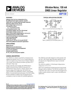
2 V to V PSRR performance of 70 dB at 10 kHz Current-limit and thermal overload protection Logic controlled enable Internal pull-down resistor on EN input 5-lead TSOT package 6-lead LFCSP package 4-ball, mm pitch WLCSP AEC-Q100 qualified for automotive applicationsAPPLICATIONS RF, voltage controlled oscillator (VCO), and phase locked loop(PLL) power supplies Mobile phones Digital camera and audio devices Portable and battery-powered equipment Post dc-to-dc regulation Portable medical devices AutomotiveTYPICAL APPLICATION CIRCUITSF igure 1. TSOT ADP151 with Fixed Output Voltage, VFigure 2. WLCSP ADP151 with Fixed Output Voltage, VFigure 3. LFCSP ADP151 with Fixed Output Voltage, VGENERAL DESCRIPTIONThe ADP151 is an Ultralow noise, low dropout (LDO) Linear regula-tor that operates from V to V and provides up to 200 mAof output current.
3 The low 135 mV dropout voltage at 200 mA loadimproves efficiency and allows operation over a wide input an innovative circuit topology, the ADP151 achieves ultralownoise performance without the necessity of a bypass capacitor,making the device ideal for noise sensitive analog and RF appli-cations. The ADP151 also achieves Ultralow noise performancewithout compromising the power supply rejection ratio (PSRR) ortransient line and load performance. The low 265 A of operatingsupply current at 200 mA load makes the ADP151 suitable forbattery-operated portable ADP151 includes an internal pull-down resistor on the ADP151 is specifically designed for stable operation withtiny 1 F, 30% ceramic input and output capacitors to meet therequirements of high performance, space constrained ADP151 is capable of 16 fixed output voltage options, rangingfrom V to and thermal overload protection circuits prevent dam-age in adverse conditions.
4 The ADP151 is available in tiny 5-leadTSOT, 6-lead LFCSP, and 4-ball, mm pitch, halide-free WLCSP packages for the smallest footprint solution to meet a variety ofportable power application SheetADP151 TABLE OF J | 2 of 1 Typical Application 3 Input and Output Capacitor, 4 Absolute Maximum 5 ESD Configurations and Function Performance of 12 Capacitor Output Voltage and Thermal 15 Thermal Circuit Board Layout 21 Ordering Voltage Products ..23 REVISION HISTORY3/2022 Rev. I to Rev. JChange to Applications to Specifications to Figure 7 Caption to Figure 12 7 Changes to Figure 13 Caption to Figure 18 8 Changes to Figure 19 Caption to Figure 21 9 Changes to Ordering Output Voltage Options 23 Data J | 3 of 23 VIN = (VOUT + V) or V, whichever is greater, VEN = VIN, IOUT = 10 mA, CIN = COUT = 1 F, and TA = 25 C, unless otherwise that VIN is the input voltage, VOUT is the output voltage, IOUT is the output current, CIN is the input capacitance, and COUT is the Conditions/ConditionsMinTypMaxUnitINPUT VOLTAGE RANGEVINTJ = 40 C to +125 SUPPLY CURRENTIGNDIOUT = 0 A10 AIOUT = 0 A, TJ = 40 C to +125 C20 AIOUT = 100 A20 AIOUT = 100 A, TJ = 40 C to +125 C40 AIOUT = 10 mA60 AIOUT = 10 mA, TJ = 40 C to +125 C90 AIOUT = 200 mA265 AIOUT = 200 mA, TJ = 40 C to +125 C350 ASHUTDOWN CURRENTIGND-SDEN = AEN = GND, TJ = 40 C to +125 AOUTPUT VOLTAGE ACCURACYVOUTIOUT = 10 mA 1+1%TSOT/LFCSPTJ = 40 C to +125 CVOUT < V100 A < IOUT < 200 mA, VIN = (VOUT + V) to V 3+2%VOUT V100 A < IOUT < 200 mA, VIN = (VOUT + V)
5 To V + = 40 C to +125 CVOUT < V100 A < IOUT < 200 mA, VIN = (VOUT + V) to V +2%VOUT V100 A < IOUT < 200 mA, VIN = (VOUT + V) to V 2+ Regulation VOUT/ VINVIN = (VOUT + V) to V, TJ = 40 C to +125 C + Regulation (TSOT/LFCSP)1 VOUT/ IOUTVOUT < VIOUT = 100 A to 200 = 100 A to 200 mA, TJ = 40 C to +125 VIOUT = 100 A to 200 = 100 A to 200 mA, TJ = 40 C to +125 Regulation (WLCSP)1 VOUT/ IOUTVOUT < VIOUT = 100 A to 200 = 100 A to 200 mA, TJ = 40 C to +125 VIOUT = 100 A to 200 = 100 A to 200 mA, TJ = 40 C to +125 VOLTAGE2 VDROPOUTIOUT = 10 mA10mVIOUT = 10 mA, TJ = 40 C to +125 C30mVTSOT/LFCSPIOUT = 200 mA150mVIOUT = 200 mA, TJ = 40 C to +125 C230mVWLCSPIOUT = 200 mA135mVIOUT = 200 mA, TJ = 40 C to +125 C200mVSTART-UP TIME3tSTART-UPVOUT = V180 sCURRENT-LIMIT THRESHOLD4 ILIMITTJ = 0 C to +125 C220300400mAData J | 4 of 23 Table Conditions/ConditionsMinTypMaxUnitW grade.
6 TJ = 40 C to +125 C205300400mAUNDERVOLTAGE LOCKOUTTJ = 40 C to +125 CInput Voltage Voltage SHUTDOWNT hermal Shutdown ThresholdTSSDTJ rising150 CThermal Shutdown HysteresisTSSD-HYS15 CEN INPUTEN Input Logic V VIN Input Logic V VIN Input Pull-Down ResistanceRENVIN = EN voltage (VEN) = OUTPUT NOISEOUTNOISE10 Hz to 100 kHz, VIN = 5 V, VOUT = V9 V rms10 Hz to 100 kHz, VIN = 5 V, VOUT = V9 V rms10 Hz to 100 kHz, VIN = 5 V, VOUT = V9 V rmsPOWER SUPPLY REJECTION RATIOPSRRVIN = VOUT + V10 kHz, VIN = V, VOUT = V, IOUT = 10 mA70dB100 kHz, VIN = V, VOUT = V, IOUT = 10 mA55dBVIN = VOUT + 1 V10 kHz, VIN = V, VOUT = V, IOUT = 10 mA70dB100 kHz, VIN = V, VOUT = V, IOUT = 10 mA55dB10 kHz, VIN = V, VOUT = V, IOUT = 10 mA70dB100 kHz, VIN = V, VOUT = V, IOUT = 10 mA55dB1 Based on an end-point calculation using mA and 200 mA loads.
7 See Figure 8 for typical load regulation performance for loads less than 1 voltage is defined as the input-to-output voltage differential when the input voltage is set to the nominal output voltage. This voltage applies only for output voltagesabove time is defined as the time between the rising edge of EN and VOUT being at 90% of its nominal threshold is defined as the current at which the output voltage drops to 90% of the specified typical value. For example, the current limit for a V outputvoltage is defined as the current that causes the output voltage to drop to 90% of V (that is, V).INPUT AND OUTPUT CAPACITOR, RECOMMENDED SPECIFICATIONST able Conditions/CommentsMinTypMaxUnitMinimum Input and Output Capacitance1 CMINTA = 40 C to +125 FCapacitor ESRRESRTA = 40 C to +125 1 The minimum input and output capacitance must be greater than F over the full range of operating conditions.
8 The full range of operating conditions in the applicationmust be considered during device selection to ensure that the minimum capacitance specification is met. X7R and X5R type capacitors are recommended, and Y5V andZ5U capacitors are not recommended for use with any low dropout (LDO) SheetADP151 ABSOLUTE MAXIMUM J | 5 of 23 Table to GND V to + VVOUT to GND V to VINEN to GND V to + VTemperature RangeStorage 65 C to +150 COperating Junction 40 C to +125 COperating Ambient 40 C to +125 CSoldering ConditionsJEDEC J-STD-020 Stresses at or above those listed under Absolute Maximum Ratingsmay cause permanent damage to the product. This is a stressrating only; functional operation of the product at these or any otherconditions above those indicated in the operational section of thisspecification is not implied. Operation beyond the maximum operat-ing conditions for extended periods may affect product DATAA bsolute maximum ratings apply individually only, not in combina-tion.
9 The ADP151 can be damaged when the junction temperaturelimits are exceeded. Monitoring ambient temperature does notguarantee that TJ is within the specified temperature limits. In appli-cations with high power dissipation and poor thermal resistance, themaximum ambient temperature may have to be applications with moderate power dissipation and low printedcircuit board (PCB) thermal resistance, the maximum ambient tem-perature can exceed the maximum limit as long as the junctiontemperature is within specification limits. TJ of the device is depend-ent on TA, the power dissipation of the device (PD), and the junctionto ambient thermal resistance of the package ( JA).To calculate the maximum TJ from TA and PD use the followingequation: TJ = TA + (PD JA)The JA of the package is based on modeling and calculation usinga 4-layer board.
10 JA is highly dependent on the application andboard layout. In applications where high maximum PD exists, closeattention to thermal board design is required. The value of JAmay vary, depending on PCB material, layout, and environmentalconditions. The specified values of JA are based on a 4-layer,4 inches 3 inches circuit board. See JESD51-7 and JESD51-9for detailed information on the board construction. For additionalinformation, see the AN-617 Application Note, MicroCSP WaferLevel Chip Scale Package. JB is the junction to board, thermal characterization parameterwith units of C/W. JB of the package is based on modelingand calculation using a 4-layer board. The JESD51-12, Guidelinesfor Reporting and Using Electronic Package Thermal Information,states that thermal characterization parameters are not the same asthermal resistances.