Transcription of LTC4370 - Two-Supply Diode-OR Current Balancing …
1 LTC437014370fTypical applicaTion FeaTuresDescripTionTwo-Supply Diode-OR Current Balancing ControllerThe LT C 4370 is a Two-Supply Current sharing controller which incorporates MOSFET ideal diodes. The diodes block reverse and shoot-through currents during start-up and fault conditions. Their forward voltage is adjusted to share the load currents between supplies. Unlike other sharing methods, neither a share bus nor trim pins on the supply are maximum MOSFET voltage drop can be set with a resistor. A fast gate turn-on reduces the load voltage droop during supply switchover. If the input supply fails or is shorted, a fast turn-off minimizes reverse Current controller operates with supplies from to 18V. For lower rail voltages, an external supply is needed at the VCC pin. Enable inputs can be used to turn off the MOSFET and put the controller in a low Current state.
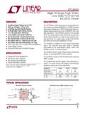
2 Status outputs indicate whether the MOSFETs are on or off. The load sharing function can be disabled to turn the LTC4370 into a dual ideal diode , 10A Load ShareCurrent Sharing Error vs Supply DifferenceapplicaTionsn Shares Load Between Two Suppliesn Eliminates Need for Active Control of Input Suppliesn No Share Bus Requiredn Blocks Reverse Currentn No Shoot-Through Current During Start-Up or Faultsn 0V to 18V High Side Operationn Enable Inputsn MOSFET On Status Outputsn Dual Ideal Diode Moden 16-Lead DFN (4mm 3mm) and MSOP Packagesn Redundant Power Suppliesn High Availability Systems and Serversn Telecom and Network InfrastructureL, LT, LT C, LT M, Linear Technology and the Linear logo are registered trademarks and PowerPath and ThinSOT are trademarks of Linear Technology Corporation. All other trademarks are the property of their respective owners. Protected by Patents, including 7920013 and 8022679.
3 Additional patent *OPTIONAL, FOR FAST TURN-ONSUM85N03-06 PGATE1 CPO1 CPO2 GNDEN1EN2 RANGE4370 FNCOUT12V, 10A39nF*39nF*VIN1 VCCFETON1 COMPFETON2 OUT1 OUT2 GATE2 VIN2 LTC43702m 2m FVINA VINB (mV) 750 20 SHARING ERROR (IVINA IVINB)/ IL (%) 10010 500 250250050020 15 55157504370 TA01bLTC437024370fabsoluTe MaxiMuM raTingsVIN1, VIN2, OUT1, OUT2 Voltages .. 2V to 24 VVCC Voltage .. to GATE1, GATE2 Voltages (Note 3) .. to 34 VCPO1, CPO2 Voltages (Note 3) .. to 34 VRANGE Voltage .. to VCC + Voltage .. to 3 VEN1, EN 2, FETON1, FETON2 Voltages .. to 24 VCPO1, CPO2 Average Current ..10mA(Notes 1, 2)1615141312111091712345678EN1 GNDVCCVIN1 GATE1 CPO1 OUT1 FETON1EN2 RANGECOMPVIN2 GATE2 CPO2 OUT2 FETON2 TOP VIEWDE PACKAGE16-LEAD (4mm 3mm) PLASTIC DFN TJMAX = 125 C, JA = 43 C/W EXPOSED PAD (PIN 17) PCB GND CONNECTION IS OPTIONAL12345678EN2 RANGECOMPVIN2 GATE2 CPO2 OUT2 FETON2161514131211109EN1 GNDVCCVIN1 GATE1 CPO1 OUT1 FETON1 TOP VIEWMS PACKAGE16-LEAD PLASTIC MSOP TJMAX = 125 C, JA = 125 C/Wpin conFiguraTionorDer inForMaTionLEAD FREE FINISHTAPE AND REELPART MARKING*PACKAGE DESCRIPTIONTEMPERATURE RANGELTC4370 CDE#PBFLTC4370 CDE#TRPBF437016-Lead (4mm 3mm) Plastic DFN0 C to 70 CLTC4370 IDE#PBFLTC4370 IDE#TRPBF437016-Lead (4mm 3mm)
4 Plastic DFN 40 C to 85 CLTC4370 CMS#PBFLTC4370 CMS#TRPBF437016-Lead Plastic MSOP0 C to 70 CLTC4370 IMS#PBFLTC4370 IMS#TRPBF437016-Lead Plastic MSOP 40 C to 85 CConsult LT C Marketing for parts specified with wider operating temperature ranges. *The temperature grade is identified by a label on the shipping more information on lead free part marking, go to: For more information on tape and reel specifications, go to: , FETON2 Currents ..5mAOperating Ambient Temper atur e Range LTC4370C ..0 C to 70 C LTC4370I .. 40 C to 85 CStorage Temper atur e Range .. 65 C to 150 CLead Temper atur e (Soldering, 10 sec) MS Package ..300 CLTC437034370felecTrical characTerisTics The l denotes those specifications which apply over the full operating temperature range, otherwise specifications are at TA = 25 C. VIN1 = VIN2 = 12V, OUT = VIN, VCC open, unless otherwise , VIN2 Operating Range With External VCC Supplyl 018 VCCV VVCC(EXT)VCC External Supply Operating RangeVIN1, VIN2 (REG)VCC Regulated , VIN2 Current Enabled, Higher Supply Enabled, Lower Supply Pull-Up Disabled Other VIN = , Both EN = 0V Other VIN = , Both EN = 0V Both VIN = 0V, VCC = 5V, Both EN = 0V Both EN = 1V l l l l 320 110 80 3 450 180 180 mA A A AICCVCC Current Enabled Disabled VCC = 5V, Both VIN = , Both EN = 0V VCC = 5V, Both VIN = , Both EN = 1V l l 2 105 220 mA AVCC(UVLO)VCC Undervoltage Lockout ThresholdVCC VCC(HYST)VCC Undervoltage Lockout Hysteresisl40120300mVLoad ShareVEA(OS)Error Amplifier Input Offsetl0 2mVgm(EA)Error Amplifier Gain ( ICOMP/ VOUT) 150 SVFR(MIN)Minimum Forward Regulation Voltage (VIN OUT)VIN = , VCC = 5V VIN = 12Vl l2 212 2525 50mV mVVFR(MAX)
5 Maximum Forward Regulation Voltage (VIN OUT)RRANGE = , VIN = , VCC = 5V RRANGE = , VIN = 12V RRANGE = , VIN = , VCC = 5V RRANGE = , VIN = 12Vl l l l40 45 425 44062 75 511 52482 100 575 590mV mV mV mVIRANGERANGE Pull-Up CurrentRANGE = 10 AVRANGE(TH)RANGE Load Share Disable ThresholdlVCC VCC VCC Drive VGATEMOSFET Gate Drive (GATE VIN) VFWD = ; I = 0, 1 A; Highest VIN = 12V VFWD = ; I = 0, 1 A; Highest VIN = l10 714 9V VtON(GATE)GATE1, GATE2 Turn-On Propagation DelayVFWD (= VIN OUT) Step: stOFF(GATE)GATE1, GATE2 Turn-Off Propagation DelayVFWD Step: sIGATE(PK)GATE1, GATE2 Peak Pull-Up Current GATE1, GATE2 Peak Pull-Down CurrentVFWD = , VGATE = 0V, CPO = 17V VFWD = 2V, VGATE = 5Vl l AIGATE(OFF)GATE1, GATE2 Off Pull-Down CurrentCorresponding EN = 1V, VGATE = AInput/Output PinsVEN(TH)EN1, EN2 Threshold VoltageEN Fallingl580600620mV VEN(TH)EN1, EN2 Threshold Hysteresisl2820mVIENEN1, EN2 CurrentAt 1 AIOUTOUT1, OUT2 Current Enabled Disabled OUTn = 0V, 12V.
6 Both EN = 0V Both EN = 1V l l 70 16 260 40 A AICPO(UP)CPO1, CPO2 Pull-Up CurrentCPO = VINl 40 70 115 AVOLFETON1, FETON2 Output Low VoltageI = 1mA I = 3mAl VVOHFETON1, FETON2 Output High VoltageI = 1 A, VFWD = 1 VlVCC VCC VCC , FETON2 Leakage CurrentAt 12Vl0 1 A VGATE(ON)MOSFET On Detect Threshold (GATE VIN)FETON Transitions perForMance characTerisTicsNote 1: Stresses beyond those listed under Absolute Maximum Ratings may cause permanent damage to the device. Exposure to any Absolute Maximum Rating condition for extended periods may affect device reliability and 2: All currents into device pins are positive; all currents out of device pins are negative. All voltages are referenced to GND unless otherwise characTerisTics TA = 25 C, VIN1 = VIN2 = 12V, OUT = VIN, VCC open, unless otherwise 3: Internal clamps limit the GATE and CPO pins to a minimum of 10V above, and a diode below the corresponding VIN pin.
7 Driving these pins to voltages beyond the clamp may damage the device. VIN Current vs VoltageOUT Current vs VoltageVIN Current vs Voltage with External VCCVCC Current vs VoltageMinimum Forward Regulation Voltage vs VIN Voltage with External VCCVIN (V)0 G01 IIN (mA)OTHER VIN = 0 VOTHER VIN = 12 VVIN (V)0 150 IIN ( A)015025012435300 10050 5010020064370 G02 VCC = 6 VOTHER VIN = 0 VVCC (V) G03 ICC (mA)BOTH VIN = 0 VVOUT (V)0 501002503612915300015050200184370 G04 IOUT ( A)VIN (V)0015301243520102554370 G05 VCC = 5 VVFR(MIN) (mV)VCC = perForMance characTerisTicsError Amplifier Transfer CharacteristicFETON Output Low Voltage vs CurrentFETON Output High Voltage vs Current VGATE Voltage vs Current VGATE and VCC Voltages vs VIN VoltageMaximum Forward Regulation Voltage vs RANGE Resistor TA = 25 C, VIN1 = VIN2 = 12V, OUT = VIN, VCC open, unless otherwise ( A)0 36 20 40 80 60 1001509312 1204370 G06 VIN = VIN (V)VIN = 18V41406210128 VIN (V)
8 06391512184370 G07 VCCVGATE VIN, VCC (V) VGATERRANGE (k )00300600204080607001004002005001004370 G08 VFR(MAX) (mV) 30030 2010 1020 VOUT1 VOUT2 (mV) 300 ICOMP ( A) 200 10010002003004370 G09 IFETON (mA)00300600124370010040020050054370 G10 VOL (mV)IFETON ( A)003 2 4 8 65142 104370 G11 VOH (V)LTC437064370fCOMP: Error Amplifier Compensation. Connect a capacitor from this pin to GND. The value of this capacitor should be approximately 10 to 50 times the gate capacitance (CISS) of the MOSFET switch. Maintain low board leakage on this pin for best load sharing accuracy. For example, 100nA of leakage Current (equal to 1V across 10M ) increases the error amplifier offset by Leave this pin open if only using ideal diode , CPO2: Charge Pump Output. Connect a capacitor from this pin to the corresponding VIN pin. The value of this capacitor should be approximately 10 the gate ca-pacitance (CISS) of the MOSFET switch.
9 The charge stored on this capacitor is used to pull up the gate during a fast turn-on. Leave this pin open if fast turn-on is not needed. EN1, EN2: Enable Input. Keep this pin below to enable sharing and diode control on the corresponding supply. Driving this pin high shuts off the MOSFET gate ( Current can still flow through its body diode). The comparator has a built-in hysteresis of 8mV. Having both EN pins high lowers the Current consumption of the device. Exposed Pad (DE Package Only): The exposed pad may be left open or connected to device ground. FETON1, FETON2: MOSFET Status Output. This pin is pulled low by an internal switch when GATE is less than above VIN to indicate an off MOSFET. Because of this, it may also signal off if small currents are flowing through a high-gm MOSFET with a large forward voltage across it. An internal 500k resistor pulls this pin up to a diode below VCC.
10 It may be pulled above VCC using an external pull-up. Tie to GND or leave open if , GATE2: MOSFET Gate Drive this pin to the gate of the external N-channel MOSFET switch. An internal clamp limits the gate voltage to 12V above, and a diode below the input supply. During fast turn-on, a pull-up Current charges GATE to CPO. During fast turn-off, a pull-down Current discharges GATE to : Device , OUT2: Output Voltage and Current Sense Input. Connect this pin to the input side of the supply s Current sense resistor. A Kelvin connection is important for ac-curate Current sharing. The voltage sensed at this pin is used to control the MOSFET gate. RANGE: Supply Differential Voltage Load Sharing Range. Connect a resistor (below 60k) from this pin to GND. A 10 A internal pull-up Current source into this resistor sets the pin voltage VRANGE. The two supplies will typi-cally share the load Current if their voltage difference is within VRANGE.