Transcription of 4-Channel, Low Noise, Low Power, 24-Bit ... - …
1 4- channel , low noise , Low Power, 24-Bit , Sigma-Delta ADC with PGA and Reference Data Sheet ad7124 -4 Rev. D Document Feedback Information furnished by analog devices is believed to be accurate and reliable. However, no responsibility is assumed by analog devices for its use, nor for any infringements of patents or other rights of third parties that may result from its use. Specifications subject to change without notice. No license is granted by implication or otherwise under any patent or patent rights of analog devices .
2 Trademarks and registered trademarks are the property of their respective owners. One Technology Way, Box 9106, Norwood, MA 02062-9106, Tel: 2015 2018 analog devices , Inc. All rights reserved. Technical Support FEATURES 3 power modes RMS noise Low power: 24 nV rms at SPS, gain = 128 (255 A typical) Mid power: 20 nV rms at SPS, gain = 128 (355 A typical) Full power: 23 nV rms at SPS, gain = 128 (930 A typical) Up to 22 noise free bits in all power modes (gain = 1) Output data rate Full power: SPS to 19,200 SPS Mid power: SPS to 4800 SPS Low power.
3 SPS to 2400 SPS Rail-to-rail analog inputs for gains > 1 Simultaneous 50 Hz/60 Hz rejection at 25 SPS (single cycle settling) Diagnostic functions (which aid safe integrity level (SIL) certification) Crosspoint multiplexed analog inputs 4 differential/7 pseudo differential inputs Programmable gain (1 to 128) Band gap reference with 10 ppm/ C drift maximum (70 A) Matched programmable excitation currents Internal clock oscillator On-chip bias voltage generator Low-side power switch General-purpose outputs Multiple filter options Internal temperature sensor Self and system calibration Sensor burnout detection Automatic channel sequencer Per channel configuration Power supply: V to V and V Independent interface power supply Power-down current: 5 A maximum Temperature range.
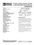
4 40 C to +125 C 32-lead LFCSP/24-lead TSSOP 3-wire or 4-wire serial interface SPI, QSPI, MICROWIRE, and DSP compatible Schmitt trigger on SCLK ESD: 4 kV APPLICATIONS Temperature measurement Pressure measurement Industrial process control Instrumentation Smart transmitters FUNCTIONAL BLOCK DIAGRAM TEMPERATURESENSORBANDGAPREFVBIASSERIALIN TERFACEANDCONTROLLOGICINTERNALCLOCKCLKSC LKDINSYNCREGCAPDIOVDDAD7124-4 AVSSDGND24-BIT - ADCX-MUXREFIN1(+)AVDDAVSSREFOUTAVDDAVSSP SWVARIABLEDIGITALFILTERDIAGNOSTICSCOMMUN ICATIONSPOWER SUPPLYSIGNAL CHAINDIGITALREFIN1( )REFIN2(+)REFIN2( ) (+)AIN7/IOUT/VBIAS/REFIN2( )13197-001 Figure 1.
5 ad7124 -4 Data Sheet Rev. D | Page 2 of 93 TABLE OF CONTENTS Features .. 1 Applications .. 1 Functional Block Diagram .. 1 Revision History .. 3 General Description .. 5 Specifications .. 6 Timing Characteristics .. 11 Absolute Maximum Ratings .. 14 Thermal Resistance .. 14 ESD Caution .. 14 Pin Configurations and Function Descriptions .. 15 Typical Performance Characteristics .. 18 Terminology .. 27 RMS noise and 28 Full Power Mode .. 28 Mid Power Mode .. 31 Low Power Mode .. 34 Getting Started .. 37 Overview.
6 37 Power Supplies .. 38 Digital Communication .. 38 Configuration Overview .. 40 ADC Circuit Information .. 45 analog Input channel .. 45 External Impedance When Using a Gain of 1 .. 46 Programmable Gain Array (PGA) .. 47 Reference .. 47 Bipolar/Unipolar Configuration .. 47 Data Output Coding .. 48 Excitation Currents .. 48 Bridge Power-Down Switch .. 49 Logic 49 Bias Voltage Generator .. 49 Clock .. 49 Power Modes .. 49 Standby and Power-Down Modes .. 49 Digital Interface .. 50 DATA _STAT U S .. 52 Serial Interface Reset (DOUT_RDY_DEL and CS_EN Bits) 52 Reset.
7 52 53 Span and Offset Limits .. 54 System Synchronization .. 54 Digital Filter .. 55 Sinc4 Filter .. 55 Sinc3 Filter .. 57 Fast Settling Mode (Sinc4 + Sinc1 Filter) .. 59 Fast Settling Mode (Sinc3 + Sinc1 Filter) .. 61 Post Filters .. 63 Summary of Filter Options .. 66 Diagnostics .. 67 Signal Chain Check .. 67 Reference Detect .. 67 Calibration, Conversion, and Saturation Errors .. 67 Overvoltage/Undervoltage Detection .. 67 Power Supply Monitors .. 68 LDO Monitoring .. 68 MCLK Counter .. 68 SPI SCLK 68 SPI Read/Write Errors.
8 69 SPI_IGNORE Error .. 69 Checksum Protection .. 69 Memory Map Checksum Protection .. 69 ROM Checksum 70 Burnout Currents .. 71 Temperature Sensor .. 71 Grounding and Layout .. 72 Applications Information .. 73 Temperature Measurement Using a Thermocouple .. 73 Temperature Measurement Using an RTD .. 74 Flowmeter .. 76 On-Chip Registers .. 78 Communications Register .. 79 Status Register .. 79 ADC_CONTROL Register .. 80 Data Register .. 82 IO_CONTROL_1 82 IO_CONTROL_2 84 ID 84 Error Register .. 84 Data Sheet ad7124 -4 Rev.
9 D | Page 3 of 93 ERROR_EN Register .. 85 MCLK_COUNT Register .. 87 channel Registers .. 87 Configuration Registers .. 89 Filter Registers .. 90 Offset Registers .. 91 Gain Registers .. 91 Outline Dimensions .. 92 Ordering Guide .. 93 REVISION HISTORY 6/2018 Rev. C to Rev. D Changes to Features Section .. 1 Changes to General Description Section .. 5 Added Table 1; Renumbered Sequentially .. 5 Changes to Drift Parameter, External REFIN Voltage Parameter, and Note 12, Ta b l e 3 .. 8 Changes to Ta b l e 7 .. 16 Changes to Figure 13 and Figure 15.
10 18 Changes to Figure 44, Figure 45, and Figure 46 .. 23 Changes to Reference Section .. 37 Changes to Accessing the ADC Register Map Section and Reset Column, Ta b l e 3 9 .. 39 Changes to External Impedance When Using a Gain of 1 Section .. 46 Changes to Reference Section .. 47 Changes to Standby and Power-Down Modes Section .. 49 Changes to Calibration Section .. 53 Change to Sinc3 Output Data Rate and Settling Time Section . 57 Change to Calibration, Conversion, and Saturation Errors Section .. 67 Changes to MCLK Counter Section.