Transcription of LT1103/LT1105 - Offline Switching Regulator
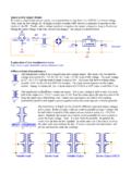
1 1LT1103/LT1105 Offline Switching RegulatorLoad RegulationDanger!! Lethal Voltages Present See Textn 1% Line and Load Regulation with No OptocouplernSwitch Frequency Up to 200kHznInternal 2A Switch and Current Sense (LT1103)nInternal 1A Totem-Pole Driver (LT1105)nStart-Up Mode Draws Only 200mAnFully Protected Against OverloadsnOvervoltage Lockout of Main SupplynProtected Against Underdrive or Overdrive to FETnOperates in Continuous or Discontinuous ModenIdeal for Flyback and Forward TopologiesnIsolated Flyback Mode Has Fully Floating OutputsThe LT 1103 Offline Switching Regulator is designed forhigh input voltage applications using an external FETswitch whose source is driven by the open collector outputof the LT1103. The LT1103 is optimized for 15W to 100 Wapplications. For higher power applications or additionalswitch current flexibility, the LT1105 is available and itstotem pole output drives the gate of an external design of the LT1103/LT1105 eliminates the needfor an optocoupler while still providing 1% load and lineregulation in a magnetic flux-sensed converter.
2 This sig-nificantly simplifies the design of Offline power suppliesand reduces the number of components which must crossthe isolation barrier to one, the LT1103/LT1105 current mode Switching techniquesare well suited to transformer isolated flyback and forwardtopologies while providing ease of frequency compensa-tion with a minimum of external components. Low exter-nal part count for a typical application combines with aFully Isolated Flyback 100kHz 50W Converter with Load Regulation CompensationIOUT (A)0 VOUT (V) to 250W Isolated Mains ConverternUp to 50W Isolated Telecom ConverternFully Isolated Multiple OutputsnDistributed Power Conversion NetworksAPPLICATIONSUTYPICAL APPLICATIONU220k1W499W39mF35V1000pF100W1 N414813k1% *50V3600mFWINDINGS FOROPTIONAL 12 VDC +LINEFILTER85 VAC TO 270 VAC+ TRANSFORMER DATA:COILTRONICS CTX110228-3L(PRI) = :NSEC = 1 :NSEC = 1 TA13*OUTPUT CAPACITOR IS THREE 1200mF, 50V CAPACITORS IN PARALLEL TO ACHIEVE REQUIRED RIPPLE CURRENT RATING AND LOW OUTPUT !
3 !HIGH VOLTAGE!!+++++, LTC and LT are registered trademarks of Linear Technology INFORMATION PURPOSES ONLYOBSOLETE:Contact Linear Technology for Potential Replacement2LT1103/LT1105200kHz maximum Switching frequency to achieve highpower density. Performance at Switching frequenciesabove 100kHz may be degraded due to internal timingconstraints associated with fully isolated flyback are the oscillator, control, and protection cir-cuitry such as current limit and overvoltage frequency and maximum duty cycle are circuitry draws 200 A for start-up of isolatedtopologies. A 5V reference as well as a 15V gate bias areavailable to power external primary-side circuitry. Noexternal current sense resistor is necessary with LT1103because it is integrated with the high current switch. TheLT1105 brings out the input to the current limit amplifierand requires the use of an external sense LT1103/LT1105 have unique features not found onother Offline Switching regulators .
4 Adaptive antisat switchdrive allows wide ranging load currents while maintaininghigh efficiency. The external FET is protected from insuf-ficient or excessive gate drive voltage with a drive detec-tion circuit. An externally activated shutdown modereduces total supply current to less than 200 A, typical forstandby operation. Fully isolated and regulated outputscan be generated in the optional isolated flyback modewithout the need for optocouplers or other isolated feed-back AND LETHAL POTENTIALS AREPRESENT IN Offline CIRCUITS!BEFORE PROCEEDING ANY FURTHER, THEREADER IS WARNED THAT CAUTION MUSTBE USED IN THE CONSTRUCTION, TESTINGAND USE OF Offline CIRCUITS. HIGHVOLTAGE, AC LINE-CONNECTED POTENTIALSARE PRESENT IN THESE CIRCUITS. EXTREMECAUTION MUST BE USED IN WORKING WITHAND MAKING CONNECTIONS TO THESECIRCUITS. REPEAT: Offline CIRCUITSCONTAIN DANGEROUS, AC LINE-CONNECTEDHIGH VOLTAGE POTENTIALS. USE TESTING PERFORMED ON AN OFFLINECIRCUIT MUST BE DONE WITH AN ISOLATIONTRANSFORMER CONNECTED BETWEEN THEOFFLINE CIRCUIT'S INPUT AND THE AC AND CONSTRUCTORS OF OFFLINECIRCUITS MUST OBSERVE THIS PRECAUTIONWHEN CONNECTING TEST EQUIPMENT TOTHE CIRCUIT TO AVOID ELECTRIC : AN ISOLATION TRANSFORMERMUST BE CONNECTED BETWEEN THE CIRCUITINPUT AND THE AC LINE IF ANY TESTEQUIPMENT IS TO BE 30 VVSW Output Voltage (LT1103).
5 50 VVSW Output Current (200ns)(LT1105) .. , FB, OSC, SS .. 6 VILIM (LT1105) .. 3V0 VLO Input Current .. 1mALead Temperature (Soldering, 10 sec.) .. 300 CMaximum Operating Ambient Temperature RangeLT1103C .. 0 C to 70 CLT1105C .. 0 C to 70 CMaximum Operating Junction Temperature RangeLT1103C .. 0 C to 100 CLT1105C .. 0 C to 100 CLT1105I .. 40 C to 125 CStorage Temperature Range .. 65 C to 150 CDESCRIPTIONUWAR I G!UUABSOLUTE MAXIMUM RATINGSWWWU(Note 1)3LT1103/LT1105 PACKAGE/ORDER INFORMATIONWUUORDER PARTNUMBERORDER PARTNUMBERTJMAX = 100 C, JA = 130 C/ W12345678 TOP VIEWGND15 VVSWILIMVINOSCFBVCN8 PACKAGE8-LEAD PDIP15 VVINOSCGNDVCFBVSWT7 PACKAGE7-LEAD TO-220 FRONT VIEW7654321 CASE IS CONNECTED TO GROUND. LEADS ARE FORMEDTJMAX = 100 C, JA = 50 C/ WConsult factory for Military grade = 100 C, JA = 100 C/W1234567 TOP VIEWN PACKAGE14-LEAD PDIPPINS 1 AND 7 MUST BE TIED TOGETHER141312111098 PWRGNDOVLOFBVC5 VSSGNDVSWNCNC15 VVINOSCILIMORDER PARTNUMBERLT1103CT7 SYMBOLPARAMETERCONDITIONSMINTYPMAXUNITSI QS upply Current8V < VIN < 30V, After Device Has Startedl102030mAISTARTS tart-Up CurrentVIN < VIN Start Thresholdl200400 AIndustrial Gradel450 AVIN Start Shutdown ThresholdNote: Switching Stops When VSW < 10V (LT1103).
6 Switching Stops When VGATE < 10V (LT1105)VREF5V Reference Line Regulation10V < VIN < VVREF Load Regulation0mA < IL < Short-Circuit CurrentCommercial Gradel2560110mAIndustrial Gradel20120mA15V Short-Circuit CurrentCommercial Gradel30130mAIndustrial Gradel25140mAVGATE15V Gate Bias Reference17 < VIN < 30V, 0mA < IL < Dropout VoltageVIN = 15V, IL = Short-Circuit Currentl3070130mASFO scillator Scaling FactorFB = 4V, VC = Open, Measured at VSW, ISW = 25mA,364044Hz FOVLO = 5V, fOSC = SF/COSC, 40kHz < fOSC < 200kHzl324048Hz FOscillator Valley Peak CHARACTERISTICSLT1105 CNLT1105 INLT1105CN8LT1105IN8 VIN = 20V, VC = , OVLO = 0V, VSW Open, TA = 25 C, unless otherwise = 20V, VC = , OVLO = 0V, VSW Open, TA = 25 C, unless otherwise CHARACTERISTICSSYMBOLPARAMETERCONDITONSM INTYPMAXUNITDCP reset Max Switch Duty CycleFB = 4V, VC = Open, fOSC = 40kHz, ISW = 25mA,l586572%(LT1103)Note: Maximum Duty Cycle Can Be Altered at OSC PinPreset Max Switch Duty CycleFB = 4V, VC = Open, fOSC = 40kHz, ISW = 25mA,l566370%(LT1105)Note.
7 Maximum Duty Cycle Can Be Altered at OSC PinIndustrial Gradel5575%OVLO ThresholdOvervoltage Lockout Threshold at Which Switching is Input Bias CurrentOVLO = 2V, Measured Out of Pin (Note 2) AVFBFB Threshold VoltageI(VC) = Input Bias CurrentFB = VFB (Note 3)l51020 AIndustrial Gradel422 AChange in FB InputFB = VFB, VC = 1V to 4V (Note 3)81113 A/VBias Current with Change in VCl71114 A/VIndustrial Gradel615 A/VFB Threshold Line Regulation10V < VIN < Amp Transconductance I(VC) = 50 A9000 12000 17500 mhol6000 12000 20000 mhoIndustrial Gradel500024000 mhoAVError Amp Voltage Gain1V < VC < 3Vl5001250V/VIndustrial Gradel450V/VVC Switching ThresholdSwitch Duty Cycle = 0% Threshold Voltagel50150250mVIndustrial Gradel50300mVError Amp Source Currentl150275 AError Amp Sink Amp Clamp VoltageFB = = Charging CurrentSS = 0Vl254060 AIndustrial Gradel2075 ASoft-Start Reset CurrentVIN = 6V, SS = Switch LeakageVSW = 45Vl500 A(LT1103)VSW = 15Vl200 ABVS witch Breakdown VoltageISW = 5mAl5070V(LT1103)VSW Current Limit (LT1103)Duty Cycle = 25% (Note 4) Switch On (LT1103) IINIQ Increase During Switch On TimeISW = to ISW(LT1103)Switch Output High LevelISW = 200mA, VGATE = (LT1105)ISW = 750mA, VGATE = Output High LevelISW = 200mA, VGATE = GradeISW = 750mA, VGATE = CHARACTERISTICSSYMBOLPARAMETERCONDITONSM INTYPMAXUNITS witch Output Low LevelISW = (LT1105)ISW = Time (LT1105)CL = 1000pF50nsFall Time (LT1105)CL = 1000pF20nsILIM Threshold Voltage (LT1105)Duty Cycle = 25% (Note 5)l300375450mVLow Switch Drive LockoutMeasured at VSW (LT1103) at 15V Gate Bias Reference (LT1105)High Switch Drive LockoutMeasured at VSW (LT1103) at 15V Gate Bias Reference (LT1105)The l denotes specifications which apply over the full operatingtemperature 1: Absolute Maximum Ratings are those values beyond which the lifeof a device may be 2.
8 The OVLO pin is clamped with a Zener and can sink amaximum input current of 3: FB input bias current changes as a function of the VC pin of change of FB input bias current is 11 A/V of change on VC. Byincluding a resistor in series with the FB pin, load regulation can be setto 4: Current limit on VSW is constant for DC < 35% and decreases forDC > 35% due to internal slope compensation circuity. The LT1103 switchcurrent limit is given by ILIM = ( DC) above 35% duty 5: The current limit threshold voltage is constant for DC < 35% anddecreases for DC > 35% due to internal slope compensation circuitry. TheLT1105 switch current limit threshold voltage is given by VLIM = ( DC) above 35% duty VOLTAGE (V)00 SUPPLY CURRENT (mA)5101520255101520LT1103 G012530 ISTARTISHUT25 CTYPICAL PERFORMANCE CHARACTERISTICS UWStart-Up Supply Current vsInput VoltageQuiescent Supply Current vsInput VoltageSupply Current vs Input VoltageINPUT VOLTAGE (V)012 QUIESCENT SUPPLY CURRENT (mA)131516172219102025LT1103 G0314202118515303540125 C25 C 55 CINPUT VOLTAGE (V)0 START-UP SUPPLY CURRENT ( A)30040050012LT1103 G0220050036915100150250350450125 C25 C 55 CVIN = 20V, VC = , OVLO = 0V, VSW Open, TA = 25 C, unless otherwise PERFORMANCE CHARACTERISTICS UWTEMPERATURE ( C) START-UP THRESHOLD (V) 252575125LT1103 G07175 50050100150 VIN Start-Up Threshold vsTemperatureVIN Shutdown Threshold vsTemperatureTEMPERATURE ( C) 75 VIN SHUTDOWN THRESHOLD (V) 252575175 50050100150 Output Switch Frequency vsTemperatureTEMPERATURE ( C) 7535 OUTPUT SWITCH FREQUENCY (kHz)
9 37414345 252550150LT1103 G0939 50075100125 COSC = 1000pFPreset Switch Maximum DutyCycle vs TemperatureSwitch Oscillator Frequency vsCapacitanceCAPACITANCE (pF)10010 SWITCH FREQUENCY (kHz)1001000100010000LT1103 G11 Overvoltage Lockout Threshold vsTemperatureTEMPERATURE ( C) 75 OVERVOLTAGE LOCKOUT THRESHOLD (V) 252575175150100500 50 TEMPERATURE ( C) 75 PRESET SWITCH DUTY CYCLE (%)697275125LT1103 G10666360 252575175150100500 50 COSC = 1000pFQuiescent Supply Current vsTemperatureShutdown Supply Current vsVC VoltageShutdown Supply Current vsInput VoltageTEMPERATURE ( C) 75 QUIESCENT SUPPLY CURRENT (mA)182022125LT1103 G04161412 50 2501752550 75 100150211917151330V8 VINPUT VOLTAGE (V)00 SHUTDOWN SUPPLY CURRENT ( A)50150200250500350102025LT1103 G051004004503005153035VC = 75mVVC = 0VC (mV)0 SHUTDOWN CURRENT ( A)300400500160LT1103 G062001000408012020050150250350450206010 014018025 C125 C 55 C7LT1103/LT1105 TYPICAL PERFORMANCE CHARACTERISTICS UW5V Reference Voltage vsTemperatureTEMPERATURE ( C) 755V REFERENCE VOLTAGE (V) 252575175 Load Regulation vsTemperatureTEMPERATURE ( C) 755V LINE REGULATION (%/ V) 252575175150100500 505V Line Regulation vsTemperature15V Gate Bias Dropout Voltage vsTemperature15V Gate Bias Reference vsTemperatureTEMPERATURE ( C) GATE BIAS REFERENCE (V) 252575125LT1103 G20175 500501001505V Reference Short-CircuitCurrent vs TemperatureTEMPERATURE ( C) 755V LOAD REGULATION (%/mA) 252575175150100500 50 TEMPERATURE ( C) 7515V GATE BIAS DROPOUT VOLTAGE (V) 252575175150100500 50 TEMPERATURE ( C) 75 INPUT BIAS CURRENT ( A) 252575125LT1103 G13175 50050100150 OVLO = 2 VOVLO Input Bias Current vsTemperatureSoft-Start Charging Current vsTemperatureTEMPERATURE ( C) 750 SOFT-START CHARGING CURRENT ( A)
10 102030405060 252575125LT1103 G14175 50050100150 TEMPERATURE ( C) 75 SOFT-START RESET CURRENT (mA)345125LT1103 G15210 252575175150100500 50 Soft-Start Reset Current vsTemperatureTEMPERATURE ( C) 755V REFERENCE SHORT-CIRCUIT CURRENT (mA)90110125LT1103 G19705030 252575175 500501001501008060408LT1103/LT1105 TYPICAL PERFORMANCE CHARACTERISTICS UW15V Gate Bias Short-CircuitCurrent vs TemperatureFB Input Bias Current vsTemperature (VC = 1V)Change in FB Input Bias Currentwith Change in VC vs Temperature(VC = 1V to 4V)TEMPERATURE ( C) 75 FEEDBACK THRESHOLD (V) 252575175150100500 50 Feedback Threshold vsTemperatureTEMPERATURE ( C) 75FB INPUT BIAS CURRENT ( A)121620125LT1103 G26840 252575175150100500 50 TEMPERATURE ( C) 757 CHANGE IN FB INPUT BIAS CURRENTWITH CHANGE IN VC ( A/ V)810111214 5050100LT1103 G2791325150175 25075125 Error Amplifier Voltage Gain vsTemperatureError Amplifier Transconductancevs TemperatureTEMPERATURE ( C) 75 ERROR AMPLIFIER TRANSCONDUCTANCE ( mho)25000125LT1103 G2815000100005000 252575175 5005010015020000 FREQUENCY (kHz) AMPLIFIER TRANSCONDUCTANCE (mho) (DEGREES)PHASEPHASE gmgmError Amplifier Transconductanceand Phase vs FrequencyTEMPERATURE ( C) 75 ERROR AMPLIFIER VOLTAGE GAIN (V/ V)2500125LT1103 G3015001000500 252575175 500501001502000 TEMPERATURE ( C) 75 LOW SWITCH DRIVE LOCKOUT THRESHOLD (V) 252575175150100500 50 Low Switch Drive LockoutThreshold vs TemperatureHigh Switch Drive LockoutThreshold vs TemperatureTEMPERATURE ( C) SWITCH DRIVE LOCKOUT THRESHOLD (V) 252575125LT1103 G24175 50050100150 TEMPERATURE ( C) 7515V GATE BIAS SHORT-CIRCUIT CURRENT (mA)90110130125LT1103 G22705030 252575175150100500 509LT1103/LT1105 CCHARA TERISTICSUWATYPICALPERFORCETEMPERATURE ( C) 75 ERROR AMPLIFIER SOURCE CURRENT ( A)