Transcription of JESD204B Clock Generator with 14 LVDS/HSTL Outputs Data ...
1 JESD204B Clock Generator with14 LVDS/HSTL OutputsData Sheet AD9528 Rev. E Document Feedback Information furnished by Analog Devices is believed to be accurate and reliable. However, no responsibility is assumed by Analog Devices for its use, nor for any infringements of patents or other rights of third parties that may result from its use. Specifications subject to change without notice. No license is granted by implication or otherwise under any patent or patent rights of Analog Devices. Trademarks and registered trademarks are the property of their respective owners.
2 One Technology Way, Box 9106, Norwood, MA 02062-9106, : 2014 2020 Analog Devices, Inc. All rights reserved. Technical Support FEATURES 14 Outputs configurable for HSTL or LVDS Maximum output frequency 6 Outputs up to GHz 8 Outputs up to 1 GHz Dependent on the voltage controlled crystal oscillator (VCXO) frequency accuracy (start-up frequency accuracy: < 100 ppm) Dedicated 8-bit dividers on each output Coarse delay: 63 steps at 1/2 the period of the RF VCO divider output frequency with no jitter impact Fine delay: 15 steps of 31 ps resolution Typical output to output skew.
3 20 ps Duty cycle correction for odd divider settings Output 12 and Output 13, VCXO output at power-up Absolute output jitter: <160 fs at MHz, 12 kHz to 20 MHz integration range Digital frequency lock detect SPI- and I2C-compatible serial control port Dual PLL architecture PLL1 Provides reference input Clock cleanup with external VCXO Phase detector rate up to 110 MHz Redundant reference inputs Automatic and manual reference switchover modes Revertive and nonrevertive switching Loss of reference detection with holdover mode Low noise LVDS/HSTL Outputs from VCXO used for radio frequency/intermediate frequency (RF/IF)
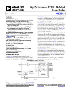
4 Synthesizers PLL2 Phase detector rate of up to 275 MHz Integrated low noise VCO APPLICATIONS high performance wireless transceivers LTE and multicarrier GSM base stations Wireless and broadband infrastructure Medical instrumentation Clocking high speed ADCs, DACs, DDSs, DDCs, DUCs, MxFEs; supports JESD204B Low jitter, low phase noise Clock distribution ATE and high performance instrumentation FUNCTIONAL BLOCK DIAGRAM PLL1 REFAREFBREF_SELCONTROLINTERFACE(SPI AND I2C)PLL2 SYSREFJESD204 BAD9528 CLOCKDISTRIBUTION14 OUTPUTSSYSREF_REQVXCO_IN12380-001 OUT0/OUT0 OUT13/OUT13 Figure 1.
5 GENERAL DESCRIPTION The AD9528 is a two-stage PLL with an integrated JESD204B SYSREF Generator for multiple device synchronization. The first stage phase-locked loop (PLL) (PLL1) provides input reference conditioning by reducing the jitter present on a system Clock . The second stage PLL (PLL2) provides high frequency clocks that achieve low integrated jitter as well as low broadband noise from the Clock output drivers. The external VCXO provides the low noise reference required by PLL2 to achieve the restrictive phase noise and jitter requirements necessary to achieve acceptable performance .
6 The on-chip VCO tunes from GHz to GHz. The integrated SYSREF Generator Outputs single shot, N-shot, or continuous signals synchronous to the PLL1 and PLL2 Outputs to time align multiple devices. The AD9528 generates six Outputs (Output 0 to Output 3, Output 12, and Output 13) with a maximum frequency of GHz, and eight Outputs with a maximum frequency of up to 1 GHz. Each output can be configured to output directly from PLL1, PLL2, or the internal SYSREF Generator . Each of the 14 output channels contains a divider with coarse digital phase adjustment and an analog fine phase delay block that allows complete flexibility in timing alignment across all 14 Outputs .
7 The AD9528 can also be used as a dual input flexible buffer to distribute 14 device Clock and/or SYSREF signals. At power-up, the AD9528 sends the VCXO signal directly to Output 12 and Output 13 to serve as the power-up ready clocks. Note that, throughout this data sheet, the dual function pin names are referenced by the relevant function where applicable. AD9528 Data Sheet Rev. E | Page 2 of 67 TABLE OF CONTENTS Features .. 1 Applications .. 1 Functional Block Diagram .. 1 General Description .. 1 Revision History .. 3 Specifications .. 4 Conditions .. 4 Supply Current.
8 4 Power Dissipation .. 5 Input Characteristics REFA, REFA, REFB, REFB, VCXO_IN, VCXO_IN, SYSREF_IN, and SYSREF_IN .. 6 PLL1 Characteristics .. 6 VCXO_VT Output Characteristics .. 7 PLL2 Characteristics .. 7 Clock Distribution Output Characteristics .. 7 Output Timing Alignment Characteristics .. 8 SYSREF_IN, SYSREF_IN, VCXO_IN, and VCXO_IN Timing Characteristics .. 8 Clock Output Absolute Phase Noise Dual Loop Mode .. 9 Clock Output Absolute Phase Noise Single Loop Mode .. 10 Clock Output Absolute Time Jitter .. 11 Clock Output Additive Time Jitter (Buffer Mode) .. 12 Logic Input Pins RESET, REF_SEL, and SYSREF_REQ.
9 12 Status Output Pins STATUS0 and STATUS1 .. 12 Serial Control Port Serial Port Interface (SPI) Mode .. 13 Serial Control Port I2C Mode .. 14 Absolute Maximum Ratings .. 15 Thermal Resistance .. 15 ESD 15 Pin Configuration and Function Descriptions .. 16 Typical performance Characteristics .. 19 Input/Output Termination Recommendations .. 22 Typical Application Circuit .. 23 Terminology .. 24 Theory of Operation .. 25 Detailed Block Diagram .. 25 Overview .. 25 Component Blocks PLL1 .. 26 Component Blocks PLL2 .. 27 Clock Distribution .. 29 SYSREF Operation .. 32 SYSREF Signal Path.
10 32 SYSREF Generator .. 34 Serial Control Port .. 35 SPI/I2C Port Selection .. 35 SPI Serial Port Operation .. 35 I2C Serial Port Operation .. 38 Device Initialization and Calibration Flowcharts .. 41 Power Dissipation and Thermal Considerations .. 46 Clock Speed and Driver Mode .. 46 Evaluation of Operating Conditions .. 46 Thermally Enhanced Package Mounting Guidelines .. 47 Control Register Map .. 48 Control Register Map Bit Descriptions .. 52 Serial Control Port Configuration (Register 0x0000 to Register 0x0001) .. 52 Clock Part Family ID (Register 0x0003 to Register 0x0006) 53 SPI Version (Register 0x000B).