Transcription of LTC2850/LTC2851/LTC2852 - 3.3V 20Mbps RS485/RS422 …
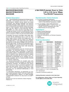
1 LTC2850/LTC2851/LTC28521285012feFor more information 20 Mbps RS485/RS422 TransceiversThe LT C 2850, LTC2851 and LTC2852 are low power, 20 Mbps RS485/RS422 transceivers operating on supplies. The receiver has a one-eighth unit load supporting up to 256 nodes per bus (C-, I-grade), and a failsafe feature that guarantees a high output state under conditions of floating or shorted driver maintains a high output impedance over the entire common mode range when disabled or when the supply is removed. Excessive power dissipation caused by bus contention or a fault is prevented by current limiting all outputs and by thermal ESD protection allows these parts to withstand up to 15kv (human body model) on the transceiver interface pins without latchup or at 20 Mbps Into 54 n Supply Voltagen 20 Mbps Maximum Data Raten No Damage or Latchup Up to 15kv HBMn High Input Impedance Supports 256 Nodes (C-, I-Grade)n Operation Up to 125 C (H-Grade)n Guaranteed Failsafe Receiver Operation Over the Entire Common Mode Rangen Current Limited Drivers and Thermal Shutdownn Delayed Micropower Shutdown: 5 A Maximum (C-, I-Grade)n Power Up/Down Glitch-Free Driver Outputsn Low Operating Current.
2 370 A Typical in Receive Moden Compatible with TIA/EIA-485-A Specificationsn Available in 8-Pin and 10-Pin 3mm 3mm DFN, 8-Pin and 10-Pin MSOP, and 8-Pin and 14-Pin SO Packagesn Low Power RS485/RS422 Transceivern Level Translatorn Backplane TransceiverVCC1 GND1 RRO1RE1DE1DI1 DRTLTC2850 LTC2850RT285012 TA01aVCC2 GND2 RRO2RE2DE2DI2 DPART NUMBERDUPLEXPACKAGELTC2850 HalfSO-8, MSOP-8, DFN-8 LTC2851 FullSO-8, MSOP-8, DFN-8 LTC2852 FullSO-14, MSOP-10, DFN-1020ns/DIV2V/DIV285012 TA01bDIABA-BL, LT, LT C, LT M, Linear Technology, the Linear logo and Module are registered trademarks of Linear Technology Corporation. All other trademarks are the property of their respective owners. LTC2850/LTC2851/LTC28522285012feFor more information MAXIMUM RATINGSS upply Voltage (VCC) .. to 7 VLogic Input Voltages (RE, DE, DI).
3 To 7 VInterface I /O: A, B, Y , Z ..(VCC 15V) to 15 VReceiver Output Voltage (RO) .. to (VCC + )(Note 1)PIN CONFIGURATIONO perating Temper atur e (Note 4) LTC285xC ..0 C to 70 C LTC285xI .. 40 C to 85 C LTC285xH .. 40 C to 125 C LTC285xMP .. 55 C to 125 CStorage Temper atur e Range .. 65 C to 150 CLead Temper atur e (Soldering, 10 sec) MSOP ..300 C LTC2850 TOP VIEWDD PACKAGE8-LEAD (3mm 3mm) PLASTIC DFN596784321 ROREDEDIVCCBAGND TJMAX = 150 C, JA = 43 C/W, JC = 3 C/W EXPOSED PAD (PIN 9) IS GND, MUST BE SOLDERED TO PCB1234 ROREDEDI8765 VCCBAGNDTOP VIEWMS8 PACKAGE8-LEAD PLASTIC MSOP TJMAX = 150 C, JA = 200 C/W, JC = 40 C/W12348765 TOP VIEWVCCBAGNDROREDEDIS8 PACKAGE8-LEAD PLASTIC SO TJMAX = 150 C, JA = 150 C/W, JC = 39 C/W LTC2851 TOP VIEWDD PACKAGE8-LEAD (3mm 3mm) PLASTIC DFN56784321 VCCRODIGNDABZY9 TJMAX = 150 C, JA = 43 C/W, JC = 3 C/W EXPOSED PAD (PIN 9)
4 IS GND, MUST BE SOLDERED TO PCB1234 VCCRODIGND8765 ABZYTOP VIEWMS8 PACKAGE8-LEAD PLASTIC MSOP TJMAX = 150 C, JA = 200 C/W, JC = 40 C/W12348765 TOP VIEWABZYVCCRODIGNDS8 PACKAGE8-LEAD PLASTIC SO TJMAX = 150 C, JA = 150 C/W, JC = 39 C/WLTC2852 TOP VIEWDD PACKAGE10-LEAD (3mm 3mm) PLASTIC DFN1011967845321 VCCABZYROREDEDIGND TJMAX = 150 C, JA = 43 C/W, JC = 3 C/W EXPOSED PAD (PIN 11) IS GND, MUST BE SOLDERED TO PCB12345 ROREDEDIGND109876 VCCABZYTOP VIEWMS PACKAGE10-LEAD PLASTIC MSOP TJMAX = 150 C, JA = 120 C/W, JC = 45 C/WTOP VIEWS PACKAGE14-LEAD PLASTIC SO1234567141312111098 NCROREDEDIGNDGNDVCCNCABZYNC TJMAX = 150 C, JA = 88 C/W, JC = 37 C/WLTC2850/LTC2851/LTC28523285012feFor more information SELECTION GUIDEORDER INFORMATIONLTC2850 CDD#TRPBFLEAD FREE DESIGNATORPBF = Lead FreeTAPE AND REELTR = Tape and ReelPACKAGE TYPEDD = 8-Lead Plastic DFN DD = 10-Lead Plastic DFN MS8 = 8-Lead Plastic MSOP MS = 10-Lead Plastic MSOP S8 = 8-Lead Plastic SO S = 14-Lead Plastic SOTEMPERATURE GRADEC = Commercial Temperature Range (0 C to 70 C) I = Industrial Temperature Range ( 40 C to 85 C) H = Automotive Temperature Range ( 40 C to 125 C) MP = Military Temperature Range ( 55 C to 125 C)
5 PRODUCT PART NUMBERLTC2850 = Half Duplex, with Enables LTC2851 = Full Duplex, No Enables LTC2852 = Full Duplex, with EnablesConsult LT C Marketing for information on non-standard lead based finish more information on lead free part marking, go to: For more information on tape and reel specifications, go to: NUMBERPART MARKINGDUPLEXLOW POWER SHUTDOWN MODEPACKAGELTC28502850/I/H, LTCQD, LCQCHalfYesSO-8, MSOP-8, DFN-8 LTC28512851/I/H, LTCWF, LCWDFullNoSO-8, MSOP-8, DFN-8 LTC28522852CS/IS/HS, LTCRX, LCRYFullYesSO-14, MSOP-10, DFN-10 LTC2850MP2850MP, LTFYD, LFYCHalfYesSO-8, MSOP-8, DFN-8 LTC2851MP2851MP, LTFYG, LFYFFullNoSO-8, MSOP-8, DFN-8 LTC2852MP2852 MPS, LTFYH, LFYJFullYesSO-14, MSOP-10, DFN-10 LTC2850/LTC2851/LTC28524285012feFor more information CHARACTERISTICS The l denotes the specifications which apply over the full operating temperature range, otherwise specifications are at TA = 25 C.
6 VCC = , unless otherwise noted. (Note 2)SYMBOLPARAMETERCONDITIONSMINTYPMAXUNIT SD river|VOD|Differential Driver Output VoltageR = , VCC = 3V (Figure 1) R = 27 , VCC = 3V (Figure 1) R = 50 , VCC = (Figure 1)l l l 2 VCC VCC VCCV V V |VOD|Difference in Magnitude of Driver Differential Output Voltage for Complementary Output StatesR = 27 or 50 (Figure 1) Common Mode Output VoltageR = 27 or 50 (Figure 1)l3V |VOC|Difference in Magnitude of Driver Common Mode Output Voltage for Complementary Output StatesR = 27 or 50 (Figure 1) Three-State (High Impedance) Output Current on Y and ZDE = 0V, (Y or Z) = 7V, 12V (LTC2852)H-Gradel l 10 50 A AIOSDM aximum Driver Short-Circuit Current 7V (Y or Z) 12V (Figure 2) l 250 180 250 300mA mAReceiverIINR eceiver Input Current (A, B)DE = TE = 0V, VCC = 0V or , VIN = 12V (Figure 3)
7 (C, I-Grade) DE = TE = 0V, VCC = 0V or , VIN = 7V, (Figure 3) (C, I-Grade)l l 100125 A ADE = TE = 0V, VCC = 0V or , VIN = 12V (Figure 3) (H-Grade) DE = TE = 0V, VCC = 0V or , VIN = 7V, (Figure 3) (H-Grade)l l 145250 A ARINR eceiver Input ResistanceRE = VCC or 0V, DE = TE = 0V, VIN = 7V, 3V, 3V, 7V, 12V (Figure 3) (C, I-Grade)l96125k RE = VCC or 0V, DE = TE = 0V, VIN = 7V, 3V, 3V, 7V, 12V (Figure 3) (H-Grade)l48125k VTHR eceiver Differential Input Threshold Voltage 7V B 12Vl VTHR eceiver Input HysteresisB = 0V25mVVOHR eceiver Output High VoltageI(RO) = 4mA, A-B = 200mV, VCC = Output Low VoltageI(RO) = 4mA, A-B = 200mV, VCC = IOZRR eceiver Three-State (High Impedance) Output Current on RORE = VCC, 0V RO VCC (LTC2850, LTC2852)l 1 AIOSRR eceiver Short-Circuit Current0V RO VCCl 85mALogicVIHL ogic Input High VoltageVCC = Input Low VoltageVCC = Input Currentl0 10 ALTC2850/LTC2851/LTC28525285012feFor more information CHARACTERISTICSNote 1: Stresses beyond those listed under Absolute Maximum Ratings may cause permanent damage to the device.
8 Exposure to any Absolute Maximum Rating condition for extended periods may affect device reliability and lifetime. High temperatures degrade operating lifetimes. Operating lifetime is derated at temperatures greater than 105 2: All currents into device pins are positive; all currents out of device pins are negative. All voltages are referenced to device ground unless otherwise specified. The l denotes the specifications which apply over the full operating temperature range, otherwise specifications are at TA = 25 C. VCC = , unless otherwise noted. (Note 2)SYMBOLPARAMETERCONDITIONSMINTYPMAXUNIT SD riverfMAXM aximum Data Rate(Note 3)l20 MbpstPLHD, tPHLDD river Input to OutputRDIFF = 54 , CL = 100pF (Figure 4)l1050ns tPDDriver Input to Output Difference |tPLHD tPHLD|RDIFF = 54 , CL = 100pF (Figure 4)l16nstSKEWDD river Output Y to Output ZRDIFF = 54 , CL = 100pF (Figure 4)l1 6nstRD, tFDDriver Rise or Fall TimeRDIFF = 54 , CL = 100pF (Figure 4) , tZHD, tLZD, tHZDD river Enable or Disable TimeRL = 500 , CL = 50pF, RE = 0V (Figure 5) (LTC2850, LTC2852)l70nstZHSD, tZLSDD river Enable from ShutdownRL = 500 , CL = 50pF, RE = VCC (Figure 5) (LTC2850, LTC2852)l8 stSHDNTime to ShutdownRL = 500 , CL = 50pF, (DE = , RE = VCC) or (DE = 0V, RE = ) (Figure 5) (LTC2850, LTC2852)
9 L100nsReceivertPLHR, tPHLRR eceiver Input to OutputCL = 15pF, VCM = , |VAB| = , tR and tF < 4ns (Figure 6)l5070nstSKEWRD ifferential Receiver Skew |tPLHR tPHLR|CL = 15pF (Figure 6)l16nstRR, tFRReceiver Output Rise or Fall TimeCL = 15pF (Figure 6) , tZHR, tLZR, tHZRR eceiver Enable/DisableRL =1k, CL =15pF, DE = VCC (Figure 7) (LTC2850, LTC2852)l50nstZHSR, tZLSRR eceiver Enable from Shutdown RL = 1k, CL = 15pF, DE = 0V (Figure 7) (LTC2850, LTC2852)l8 sNote 3: Maximum data rate is guaranteed by other measured parameters and is not tested 4: This IC includes overtemperature protection that is intended to protect the device during momentary overload conditions. Overtemperature protection activates at a junction temperature exceeding 150 C. Continuous operation above the specified maximum operating junction temperature may result in device degradation or CHARACTERISTICS The l denotes the specifications which apply over the full operating temperature range, otherwise specifications are at TA = 25 C.
10 VCC = , unless otherwise noted. (Note 2)SYMBOLPARAMETERCONDITIONSMINTYPMAXUNIT SS uppliesICCSS upply Current in Shutdown ModeDE = 0V, RE = VCC, LTC2850, LTC2852 (C and I-Grade) LTC2850, LTC2852 (H-Grade)l l0 05 15 A AICCRS upply Current in Receive ModeDE = 0V, RE = 0V (LTC2850, LTC2852)l370900 AICCTS upply Current in Transmit ModeNo Load, DE = VCC, RE = VCC (LTC2850, LTC2852)l4501000 AICCTRS upply Current with Both Driver and Receiver EnabledNo Load, DE = VCC, RE = 0Vl4501000 ALTC2850/LTC2851/LTC28526285012feFor more information CIRCUITS +DRIVERDIGNDORVCCR285012 F01 YZRVOC +VODF igure 1. Driver DC CharacteristicsFigure 2. Driver Output Short-Circuit CurrentFigure 3. Receiver Input Current and Input ResistanceFigure 4. Driver Timing MeasurementDRIVERDIGNDORVCC285012 F02YZ+ IOSD 7V TO 12V+ RECEIVER285012 F03A OR BVINIINB OR AVINIINRIN = DRIVERDIRDIFFCLCL285012 F04aYZ1/2 VO90%90%0010%285012 F04b10%VOVCCY, ZDI(Y-Z)0 VtSKEWDtPLHDtRDtFDtPHLDLTC2850/LTC2851/L TC28527285012feFor more information 5.