The Output Impedance From Switched Dc
Found 10 free book(s)
Choose the right data converter for your application
www.ti.comO) output impedance, V OUT will drop momentarily when cap load is switched. • As the output recovers, ringing may occur, which results in increased settling time. • Use external R: isolates OpAmp output from capacitive load and improves settling. Cs S/H R R …
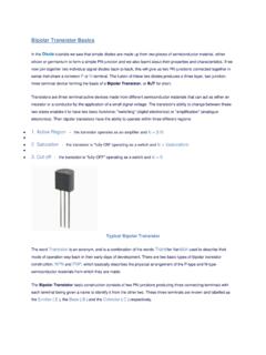
Bipolar Transistor BJT
www.pitt.eduPN-junction, while the output impedance is HIGH as it is taken from a reverse-biased PN-junction. ... through the device between the collector and the emitter terminals when the transistor is switched "fully-ON". ... DC Current Gain.
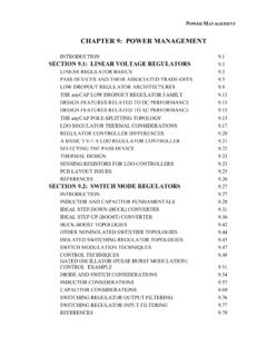
CHAPTER 9: POWER MANAGEMENT - Analog Devices
www.analog.comDESIGN FEATURES RELATED TO DC PERFORMANCE 9.13 ... REGULATOR OUTPUT SWITCHED CAPACITOR VOLTAGE CONVERTERS 9.92 . POWER MANAGEMENT INTRODUCTION 9.1 ... All of the three connections C/D/E have the characteristic of high output impedance, and require an output capacitor for stability. The fact that the output cap is part …
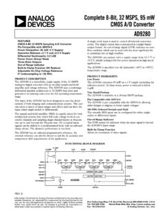
a Complete 8-Bit, 32 MSPS, 95 mW CMOS A/D Converter …
www.analog.comIN 1 pF Switched Aperture Delay t AP 4ns Aperture Uncertainty (Jitter) t AJ 2ps Input Bandwidth (–3 dB) BW Full Power (0 dB) 300 MHz DC Leakage Current 43 µA Input = ±FS INTERNAL REFERENCE Output Voltage (1 V Mode) VREF 1 V REFSENSE = VREF Output Voltage Tolerance (1 V Mode) ±10 ±25 mV Output Voltage (2 V Mode) VREF 2 V REFSENSE = GND

Introduction to Switched-Capacitor Circuits
www.seas.ucla.eduIntroduction to Switched-Capacitor Circuits Our study of amplifiers in previous chapters has dealt with only cases where the input signal is continuously available and applied to the circuit and the output signal is continuously observed. Called “continuous-time” circuits, such amplifiers find wide application in audio, video, and high-
33609/JD Limiter/Compressor
www.thehistoryofrecording.comTR9, TR13 and TR1 gives a low output impedance signal equal to the larger of the compressor or limiter sidechain signals. The voltage is attenuated by R36, RV2, R45, R29 and D10 supplied as the control voltage to the diode bridge. Limiting The output of the power amplifier board (10340-C) is connected via the limit in (Plug 3, pin 1; P3

A CAN Physical Layer Discussion
ww1.microchip.comDC Voltage on CANH and CANL -3 +32 -40 +40 V Exceeds ISO-11898 ... switched off and the receiver operates in a reduced power mode. While the receive pin (RXD) is still functional, it will operate at a slower rate. ... CANL pins remain in the high impedance state until VDD). High.
Electric Motors and Drives
www.emic-bg.orgConverter output impedance: overlap 141 Four-quadrant operation and inversion 143 Single-converter reversing drives 144 Double SP-converter reversing drives 146 Power factor and supply effects 146 Control Arrangements for D.C. Drives 148 Current control 150 Torque control 152 Speed control 152 Overall operating region 154 Armature voltage ...
A CAN Physical Layer Discussion
ww1.microchip.comDC Voltage on CANH and CANL -3 +32 -40 +40 V Exceeds ISO-11898 ... switched off and the receiver operates in a reduced power mode. While the receive pin (RXD) is still functional, it will operate at a slower rate. ... CANL pins remain in the high impedance state until VDD). High.
Class E/F Amplifiers - University of California, Berkeley
rfic.eecs.berkeley.eduNormalized Output Power It’s easy to show that for Class A/B/C amplifiers, the efficiency and output power are given by: It’s useful to normalize the output power versus the product of V bk and I max (I dc) EECS 242 Prof. Ali M. Niknejad (C) 2009