Search results with tag "Glitch"

PCA9539; PCA9539R - NXP
www.nxp.com16-bit I2C-bus and SMBus low power I/O port with interrupt and reset Polarity inversion register Active LOW interrupt output Active LOW reset input Low standby current Noise filter on SCL/SDA inputs No glitch on power-up Internal power-on reset 16 I/O pins which default to 16 inputs 0 Hz to 400 kHz clock frequency

PCA9535 PCA9535C 16-bit I2C-bus and SMBus, low power I/O ...
www.nxp.com16-bit I2C-bus and SMBus, low power I/O port with interrupt No glitch on power-up Internal power-on reset 16 I/O pins which default to 16 inputs 0 Hz to 400 kHz clock frequency ESD protection exceeds 2000 V HBM per JESD22-A114, 200 V MM per JESD22-A115, and 1000 V CDM per JESD22-C101
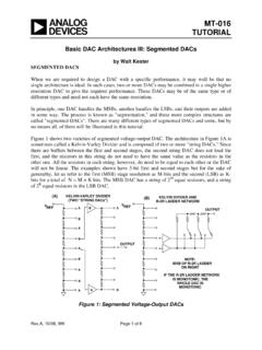
MT-016: Basic DAC Architectures III: Segmented DACs
www.analog.comlatches are required to implement this ultra low glitch architecture. The basic current switching cell in the TxDAC family is made up of a differential PMOS transistor pair as shown in Figure 6. The differential pairs are driven with low-level logic to minimize switching transients and time skew. The DAC outputs are symmetrical differential

NI 6229 Device Specifications - National Instruments
www.ni.comPower-off glitch 400 mV for 200 ms Output FIFO size 8,191 samples shared among channels used Data transfers PCI/PXI DMA (scatter-gather), interrupts, ... Output low current (IOL) PFI <0..15>/P1/P2 -— 16 mA Table 4. USB Devices Level Minimum Maximum Input …

TCA9548A Low-Voltage 8-Channel I2C Switch with Reset ...
www.ti.com• Low RON switches • Allows voltage-level translation between 1.8-V, 2.5-V, 3.3-V, and 5-V buses • No glitch on power up • Supports hot insertion • Low standby current • Operating power-supply voltage range of 1.65 V to 5.5 V • 5-V Tolerant inputs • 0- to 400-kHz Clock frequency • Latch-up performance exceeds 100 mA Per JESD ...

Coding And Scripting Techniques For FSM Designs With ...
www.sunburst-design.comCoding And Scripting Techniques For FSM Designs With Synthesis-Optimized, Glitch-Free Outputs Clifford E. Cummings Sunburst Design, Inc. ABSTRACT
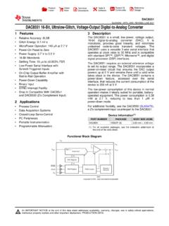
DAC8551 16-Bit, Ultralow-Glitch, Voltage-Output Digital to ...
www.ti.comout dac v dd in

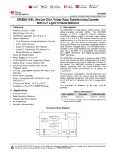
DAC8550 16-Bit, Ultra-Low Glitch, Voltage Output …
www.ti.comV DD V OUT Shift Register GND SYNC SCLK D IN DAC Register 16-Bit DAC 16 16 V REF REF (+) PWB Control Resistor Network V FB Copyright © 2016, Texas Instruments Incorporated Product Folder
DAC8560 16-Bit, Ultra-Low Glitch, Voltage Output …
www.ti.comDAC Register 16 16-Bit DAC Ref (+) 2.5V Reference V DD V OUT V FB V REF Shift Register GND SYNC SCLK D IN PWD Control Resistor Network 16 Product Folder Order Now Technical Documents Tools &

Glitch Protocol // Ecosystem
glitch.financedApps are designed to work within the ecosystem (eg. dynamic, loose or firm rules around white-labeling addresses) came down to what role they play in DeFi and how they should be shaped by the key stakeholders. In this picture, we see there being three key stake-holders: users, developers, and enablers.
Similar queries
PCA9539; PCA9539R, Glitch, Basic DAC Architectures III: Segmented DACs, Low Glitch, Designs With Synthesis-Optimized, Glitch-Free Outputs, Bit, Ultralow-Glitch, Voltage-Output Digital, DAC8550 16-Bit, Ultra-Low Glitch, Voltage Output, 16 16, Texas Instruments, DAC8560 16, Ultra, Voltage Output, Glitch Protocol // Ecosystem, The ecosystem, They