Search results with tag "Voltage output"
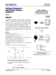
LM337 - Voltage Regulator - Adjustable Output, Negative
www.onsemi.comVoltage Regulator - Adjustable Output, Negative 1.5 A LM337 The LM337 is an adjustable 3−terminal negative voltage regulator capable of supplying in excess of 1.5 A over an output voltage range of −1.2 V to −37 V. This voltage regulator is exceptionally easy to use and requires only two external resistors to set the output voltage.
Adjustable Output, Positive D2PAK 3 D2T SUFFIX CASE 936
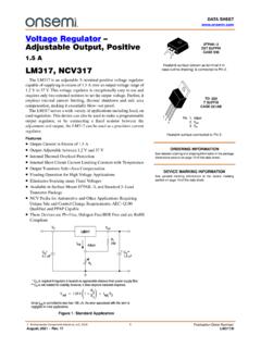
www.onsemi.comVoltage Regulator – Adjustable Output, Positive 1.5 A LM317, NCV317 The LM317 is an adjustable 3−terminal positive voltage regulator capable of supplying in excess of 1.5 A over an output voltage range of 1.2 V to 37 V. This voltage regulator is exceptionally easy to use and requires only two external resistors to set the output voltage ...
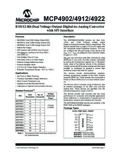
MCP4902/4912/4922 Data Sheet - Microchip Technology
ww1.microchip.com• MCP4902: Dual 8-Bit Voltage Output DAC • MCP4912: Dual 10-Bit Voltage Output DAC • MCP4922: Dual 12-Bit Voltage Output DAC • Rail-to-Rail Output • SPI Interface with 20 MHz Clock Support • Simultaneous Latching of the Dual DACs with LDAC pin • Fast Settling Time of 4.5 µs • Selectable Unity or 2x Gain Output

LM2931 - LDO Voltage Regulator - Adjustable Output, …
www.onsemi.comThe LM2931 series consists of positive fixed and adjustable output voltage regulators that are specifically designed to maintain proper regulation with an extremely low input−to−output voltage differential. These devices are capable of supplying output currents in excess of 100 mA and feature a low bias current of 0.4 mA at 10 mA output.
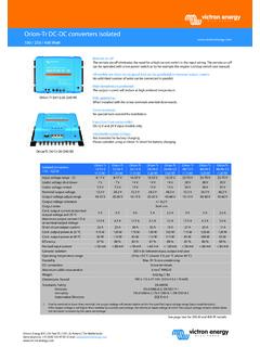
Orion-Tr DC-DC converters isolated - Victron Energy
www.victronenergy.comOutput voltage adjust range 10-15V 20-30V 10-15V 20-30V 40-60V 10-15V 20-30V 40-60V Output voltage tolerance +/- 0,2V Output noise 2 mV rms Cont. output current at nominal output voltage and 40 °C 30A 15A 30A 17A 8,5A 30A 16A …

NCP13992 - Current Mode Resonant Controller with ...
www.onsemi.comDRIVER OUTPUTS tr Output voltage rise−time @ CL = 1 nF, 10−90% of output signal 12, 14 20 45 80 ns tf Output voltage fall−time @ CL = 1 nF, 10−90% of output signal 12, 14 5 30 50 ns ROH Source resistance 12, 14 4 16 32 ROL Sink resistance 12, 14 1 5 11 IDRVSOURCE Output high short circuit pulsed current VDRV = 0 V, PW 10 s 12, 14 − 0 ...

Typical Application - SparkFun Electronics
www.sparkfun.comOutput voltage proportional to AC or DC currents Factory-trimmed for accuracy Extremely stable output offset voltage Nearly zero magnetic hysteresis Ratiometric output from supply voltage Fully Integrated, Hall Effect-Based Linear Current Sensor with 2.1 kVRMS Voltage Isolation and a Low-Resistance Current Conductor
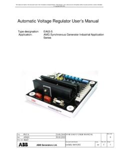
Automatic Voltage Regulator User’s Manual - ABB
library.e.abb.comVoltage: 30-260 VAC. Frequency: 40-500 Hz. Output Voltage: 85 VDC at 110 VAC input. 170 VDC at 220 VAC input. Current: continuous 5 ADC. maximum 40 ADC. Voltage bu ilt-up Residual voltage >5 VAC at 25 Hz. Voltage adjustment <1.0 % (engine speed variation within 4 %). Excitation resistance >9 . Current compensation 1 or 5 A>0.2 VA (SW2 selectable).

LM555 Timer datasheet (Rev. D) - Texas Instruments
www.ti.comTrigger Current 0.5 0.9 μA Reset Voltage 0.4 0.5 1 V Reset Current 0.1 0.4 mA Threshold Current (5) 0.1 0.25 μA Control Voltage Level VCC = 15 V 9 10 11 V VCC = 5 V 2.6 3.33 4 Pin 7 Leakage Output High 1 100 nA Pin 7 Sat (6) Output Low VCC = 15 V, I7 = 15 mA 180 mV Output Low VCC = 4.5 V, I7 = 4.5 mA 80 200 mV Output Voltage Drop (Low) VCC = 15 V
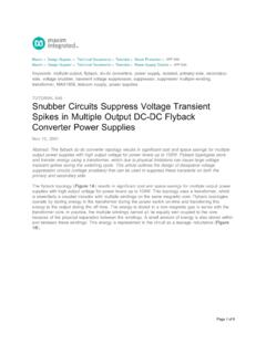
Snubber Circuits Suppress Voltage Transient Spikes in ...
pdfserv.maximintegrated.comthe output capacitance, COSS, of the MOSFET form a parasitic LC network. The peak voltage is given by: VPEAK = IP (√(LLP/(CP+COSS))) + VIN + VOUT/N Where IP is the current level circulating at the time the MOSFET turns OFF, N is the ratio of secondary to primary turns, VIN is the input voltage, and VOUT is the output voltage.

Operational Amplifier Circuits
ocw.mit.eduThe output voltage Vout is a sum of the input voltages with weighting factors given by the values of the resistors. If the input resistors are equal R1=R2=R3=R, Equation (1.3) becomes out (in12in in3 RF VVVV) R =− + + (1.4) The output voltage is thus the sum of the input voltages with a …

LMC7660 Switched Capacitor Voltage Converter datasheet ...
www.ti.comthe available output voltage and increased the output series resistance. The TI LMC7660 has been designed to solve the inherent latch problem. The LCM7660 can operate over the entire supply voltage and temperature range without the need for an output diode. When replacing existing designs, the LMC7660 can be operated with diode Dx.

250 MHz, Voltage Output, 4-Quadrant Multiplier Data …
www.analog.comis a complete four-quadrant, voltage output analog multiplier, fabricated on an advanced dielectrically isolated complementary bipolar process. It generates the linear product of its X and Y voltage inputs with a −3 dB output bandwidth of 250 MHz (a …
Lecture Notes for Analog Electronics - University of Oregon
pages.uoregon.eduTH! 0 the output voltage delivered to the load RL remains at constant voltage. For nite R TH, the output voltage is reduced from V TH by an amount IR TH,whereIis the current of the complete circuit, which depends upon the value of the load resistance RL: I = V TH=(R TH +RL). Therefore, R TH determines to what extent the output of the rst ...

How to Generate a Negative Voltage Using Buck Converters?
www.aosmd.comFigure 2: Buck type converter to generate negative voltage Since this circuit is a buck type converter and IC ground (virtual ground) is equal to output voltage which is the most negative voltage, there is no need for additional amplifier to generate the positive voltage and there is no potential damage of ESD diode using buck-boost type converter.
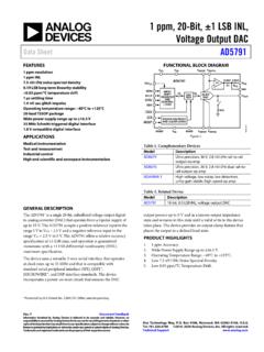
1 ppm, 20-Bit, ±1 LSB INL, Voltage Output DAC
www.analog.com18-bit, 0.5 LSB INL, voltage output DAC . GENERAL DESCRIPTION The AD5791 1 is a single 20-bit, unbuffered voltage -output digital-to-analog converter ( DAC) that operates from a bipolar supply of up to 33 V. The AD5791 accepts a positive reference input in the range 5 V to V DD − 2.5 V and a negative reference input in the
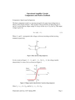
Operational Amplifier Circuits Comparators and Positive ...
ocw.mit.eduThe voltage V+ is related to the output voltage V o by the simple voltage divider formed by resistors R1 and R2. V+ = V R1 (1.7) o RR 1 + 2 Note that V+ depends on the output voltage V o and the in turn V o depends on the difference between V+ and V−: V o = A V (+ −V −) The key to analyzing these positive feedback circuits is to assume an ...

MT-041: Op Amp Input and Output Common-Mode and ...
www.analog.cominput and the output voltage ranges—especially during the op amp selection process. OUTPUT COMMON-MODE VOLTAGE RANGE . Figure 1 below is a general illustration of the limitations imposed by input and output dynamic ranges of an op amp, related to both supply rails. Any op amp will always be powered by two
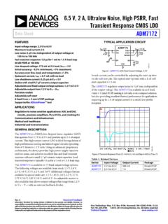
6.5 V, 2 A, Ultralow Noise, High PSRR, Fast Transient ...
www.analog.comADM7172 with Fixed Output Voltage, 3.3 V Inrush current can be controlled by adjusting the start-up time via the soft start pin. The typical start-up time with a 1 nF soft start capacitor is 1.0 ms. The . ADM7172 regulator output noise is 5 μV rms, independent of the output voltage. The ADM7172 is available in an 8-lead,
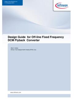
Design Guide for Off-line Fixed Frequency DCM Flyback ...
www.mouser.comusually occurs for designs wherein the output voltage is low and output current is relatively high (> 6A), typically for output power over 50W, though for 5V or lower outputs this is a problem at power below 50W. Table 1: DCM vs CCM Figure 2: CCM and DCM Flyback Current Waveforms Figure 1: Flyback Schematic
Federal Pacific Medium Voltage Transformer Catalog
federalpacific.coma distribution transformer as having an input of 34.5 kV or less, an output voltage of 600 volts or less, 60 Hz and 15 KVA to 2500 kVA. Transformers Exempt from Efficiency Requirements • Transformers with output voltages greater than 600 volt • Transformers outside the kVA range of 15 to 2500 or not defined in the tables above
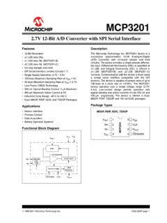
MCP3201 - 2.7V 12-Bit A/D Converter with SPI Serial ...
ww1.microchip.comMCP3201 DS21290F-page 4 1998-2011 Microchip Technology Inc. TEMPERATURE CHARACTERISTICS High Level Output Voltage V OH 4.1 — — V IOH = -1 mA, VDD = 4.5V Low Level Output Voltage VOL —— 0.4 VIOL = 1 mA, VDD = 4.5V Input Leakage Current I LI-10 — 10 µA VIN = VSS or VDD Output Leakage Current I LO-10 — 10 µA …
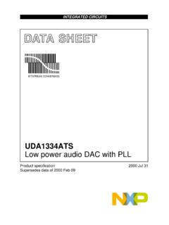
UDA1334ATS Low power audio DAC with PLL - NXP
www.nxp.com5 QUICK REFERENCE DATA Note 1. The output voltage of the DAC scales proportionally to the power supply voltage. SYMBOL PARAMETER CONDITIONS MIN. TYP. MAX. UNIT Supplies VDDA DAC analog supply voltage 2.4 3.0 3.6 V VDDD digital supply voltage 2.4 3.0 3.6 V IDDA DAC analog supply current audio mode − 3.5 − mA video mode − 3.5 − mA

LM324 - Single Supply Quad Operational Amplifiers
www.onsemi.comlm324, lm324a, lm324e, lm224, lm2902, lm2902e, lm2902v, ncv2902 www.onsemi.com 7 v or, output voltage range (v ) pp v o, output voltage (mv) 14 12 10 8.0

High Voltage FET-Input Operational Amplifier …
www.ti.comSBOS156B − MARCH 1987 − REVISED APRIL 2008 www.ti.com 6 TYPICAL CHARACTERISTICS (continued) At TA = +25°C and VS = ±40V, unless otherwise noted. OUTPUT VOLTAGE SWING vs OUTPUT CURRENT (V+) (V+) − 2
250 MHz, Voltage Output, 4-Quadrant Multiplier Data Sheet ...
www.analog.comAD835. is a four-quadrant, voltage output analog multiplier, ( )( ) Z + − − =, , , + + presumed expressed in V, are used throughout this data sheet to

LTM2881 - Completed Isolated RS485/RS422 µModule ...
www.analog.comn Industrial Networks n Breaking RS485 Ground Loops ... VOC Driver Common Mode Output Voltage R = 27Ω or R = 50Ω (Figure 1) l 3 V ∆ ... for Complementary Output States R = 27Ω or R = 50Ω (Figure 1) l 0.2 V IOZD Driver Three-State (High Impedance) Output Current on Y and Z DE = 0V, (Y or Z) = –7V, +12V DE = 0V, (Y or Z) = –7V, +12V, H ...
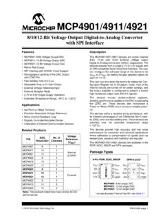
8/10/12-Bit Voltage Output Digital-to-Analog Converter ...
ww1.microchip.com8-bit, 10-bit and 12-bit buffered voltage output Digital-to-Analog Converters (DACs), respectively. The devices operate from a single 2.7V to 5.5V supply with an SPI compatible Serial Peripheral Interface. The user can configure the full-scale range of the device to be VREF or 2*VREF by setting the gain selection option bit (gain of 1 of 2).

INTERLEAVED BOOST CONVERTER - IJEETC
www.ijeetc.comThe boosting ratio of the converter is a function of the duty ratio. It is same as in conventional ... high commutation speed and high efficiency at low voltages. Parameter Symbol Value Unit Input Voltage V in 60 15 V ... The waveforms for the output voltage and current through the inductors L …
LM358 - Diodes Incorporated
www.diodes.com• In the linear mode the input common-mode voltage range includes ground and the output voltage can also swing to ground, whilst operating from only a single power supply voltage. • The unity gain crossing frequency is temperature compensated. • The input bias current is temperature compensated. Notes: 1. EU Directive 2002/95/EC (RoHS).

Datasheet - L78M - Precision 500 mA regulators
www.st.comJun 06, 2007 · VO Output voltage 5.75 6 6.25 V VO Output voltage IO = 5 to 350 mA, VI = 8 to 21 V 5.7 6 6.3 V ∆VO Line regulation VI = 8 to 25 V, IO = 200 mA 100 mV VI = 9 to 25 V, IO = 200 mA 50 ∆VO Load regulation IO = 5 to 500 mA, TJ = 25 °C 120 mV IO = 5 to 200 mA, TJ = 25 °C 60 Id Quiescent current 6 mA ∆Id Quiescent current change IO = 5 to 350 ...

TSSOP8 SO8 LM2904W, LM2904AW Description LM2904, …
www.st.com• Large output voltage swing 0 V to [(VCC +) -1.5 V] ... independent of the magnitude of the power supply voltage. Application areas include transducer amplifiers, DC gain blocks and all the ... The maximum output current is approximately 40 mA, independent of the magnitude of V.

RF Amplifier Output Voltage, Current, Power, and Impedance ...
www.arworld.usvoltage, current, and power of a 50 Ω amplifier operating under ideal conditions. Assume we have a 100 watt amplifier with 50 Ω output impedance driving a 50 Ω load. This is an ideal situation in that 100% of the forward power will be absorbed in the load
74HC14; 74HCT14 • JESD8C (2.7 V to 3.6 V) • JESD7A (2.0 V ...
assets.nexperia.com[1] The input and output voltage ratings may be exceeded if the input and output current ratings are observed. [2] For SOT108-1 (SO14) package: P tot derates linearly with 10.1 mW/K above 100 °C. For SOT402-1 (TSSOP14) package: P tot derates linearly with 7.3 mW/K above 81 °C.

LM1117 - 800 mA Low-Dropout Linear Regulator
www.onsemi.comThe LM1117 is a low dropout voltage regulator with a dropout of 1.2 V at 800 mA of load current. The LM1117 is available in an adjustable version, which can set the output voltage from 1.25 to 13.8 V with only two external resistors. In addition, it …

Understanding LED Drivers - 1000Bulbs.com
www.1000bulbs.comamps, and less than 100 watts. However, these limitations pose restrictions on the number of LEDs a Class 2 driver can operate. UL Class 1 drivers have output ranges outside UL Class 2 designations. An LED Driver with a UL Class 1 rating has a high-voltage output and safety protection is required within the fixture. A Class 1 driver can

XII. AC Circuits - Worked Examples
web.mit.eduExample 4: High-pass RL filter A high-pass RL filter can be represented by the circuit in the figure below, with r being the internal resistance of the inductor. (a) Find V, the ratio of the maximum output voltage V to the maximum input voltage V. out,0 /Vin,0 in,0 out,0 (b) Let r =20.0 Ω, R=5.0 Ω, and L=250 mH.What is the frequency if ,0,0

Multiple Range, 16-/12-Bit, Bipolar/Unipolar Voltage ...
www.analog.comMultiple Range, 16-/12-Bit, Bipolar/Unipolar Voltage Output DACs with 2 ppm/°C Reference Data Sheet AD5761R/AD5721R Rev. C Document Feedback Information furnished by Analog Devices is believed to be accurate and reliable.

DAC8550 16-Bit, Ultra-Low Glitch, Voltage Output …
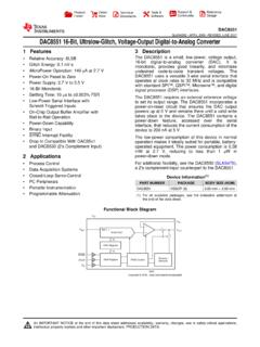
www.ti.comV DD V OUT Shift Register GND SYNC SCLK D IN DAC Register 16-Bit DAC 16 16 V REF REF (+) PWB Control Resistor Network V FB Copyright © 2016, Texas Instruments Incorporated Product Folder
DAC8551 16-Bit, Ultralow-Glitch, Voltage-Output …
www.ti.comout dac v dd in
16-BIT,LOW POWER, VOLTAGE OUTPUT, I C …
www.ti.com3 mm x 5 mm www .ti.com FEATURES DESCRIPTION APPLICATIONS _ 16 Bit DAC + DAC Register I2C Block Power Down Control Logic Resistor Network 16 Ref + VREF VDD SDA SCL A0 GND V(SENSE) VOUT Temporary Register
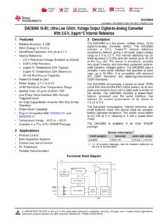
DAC8560 16-Bit, Ultra-Low Glitch, Voltage Output …
www.ti.comDAC Register 16 16-Bit DAC Ref (+) 2.5V Reference V DD V OUT V FB V REF Shift Register GND SYNC SCLK D IN PWD Control Resistor Network 16 Product Folder Order Now Technical Documents Tools &

Analog Multiplier Data Sheet AD633 - Analog Devices
www.analog.comAD633 is a functionally complete, four-quadrant, analog multiplier. It includes high impedance, differential X and Y inputs, and a high impedance summing input (Z). The low impedance output voltage is a nominal 10 V full scale provided by a buried Zener. The AD633 is the first product to offer these features in

Voltage Output Temperature Sensor with Signal Conditioning ...
www.analog.comThe output voltage is proportional to the temperature x the supply voltage (ratiometric). The output swings from 0.25 V at −50°C to +4.75 V at +150°C using a single +5.0 V supply. Due to its ratiometric nature, the AD22100 offers a cost-effective solution when interfacing to an analog-to-digital converter.
Voltage Output Temperature Sensor with Signal …
www.analog.comVoltage Output Temperature Sensor with Signal Conditioning AD22100 Rev. D Information furnished by Analog Devices is believed to be accurate and reliable.
Similar queries
Voltage, Output, Output voltage, MCP4902/4912/4922, Voltage Output, LDO Voltage Regulator - Adjustable Output,, Current, Driver, Application, SparkFun Electronics, Texas Instruments, Voltage Output, 4-Quadrant Multiplier, Quadrant, Multiplier, Negative voltage, Output digital, To-analog, Regulator output, Serial, Output Voltage V, Input, DATA, Single Supply Quad, 10 8, Voltage Output, 4-Quadrant Multiplier Data Sheet, Data sheet, Industrial, Output current, Bit Voltage Output Digital-to-Analog Converter, Boosting, High, Transducer, Understanding, Limitations, XII. AC Circuits - Worked Examples, Bipolar, DAC8550 16-Bit, Ultra-Low Glitch, Voltage Output, 16 16, Bit, Ultralow-Glitch, Voltage-Output, Www .ti.com, DAC8560 16, Ultra, Low Glitch, Multiplier Data, Analog Devices