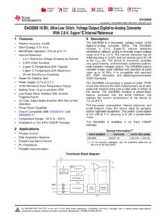
Transcription of DAC8550 16-Bit, Ultra-Low Glitch, Voltage Output …
1 Product Order Technical Tools & Support & Reference Folder Now Documents Software Community Design DAC8550 . SLAS476H MARCH 2006 REVISED JUNE 2017. DAC8550 16-bit, Ultra-Low glitch , Voltage Output Digital-To-Analog Converter 1 Features 3 Description . 1 Relative Accuracy: 8 LSB The DAC8550 is a small, low-power, Voltage Output , 16-bit digital-to-analog converter (DAC). It is glitch Energy: nV-s monotonic, provides good linearity, and minimizes MicroPower Operation: 140 A at V undesired code-to-code transient voltages. The Power-On Reset to Midscale DAC8550 uses a versatile, 3-wire serial interface that Power Supply: V to V operates at clock rates of up to 30 MHz and is compatible with standard SPI , QSPI , 16-Bit Monotonic Microwire , and digital signal processor (DSP).
2 Settling Time: 10 s to FSR interfaces. Low-Power Serial Interface with Schmitt-Triggered The DAC8550 requires an external reference Voltage Inputs to set its Output range. The DAC8550 incorporates a On-Chip Output Buffer Amplifier with Rail-to-Rail power-on reset circuit that ensures that the DAC. Output Amplifier Output powers up at midscale and remains there until a valid write takes place to the device. The DAC8550 . Power-Down Capability contains a power-down feature, accessed over the 2's Complement Input serial interface, that reduces the current consumption SYNC Interrupt Facility of the device to 200 nA at 5 V.
3 Drop-In Compatible with DAC8531/01 and The low-power consumption of this device in normal DAC8551 (Binary Input) operation makes it ideal for portable, battery-operated Available in a Tiny MSOP-8 Package equipment. Power consumption is mW at V, reducing to less than 1 W in power-down mode. 2 Applications The DAC8550 is available in an MSOP-8 package. Process Control For additional flexibilty, see the DAC8551, a binary- Data Acquisition Systems coded counterpart to the DAC8550 . Closed-Loop Servo-Control Device Information(1).
4 PC Peripherals PART NUMBER PACKAGE BODY SIZE (NOM). Portable Instrumentation DAC8550 VSSOP (8) mm mm Programmable Attenuation (1) For all available packages, see the orderable addendum at the end of the data sheet. Functional Block Diagram VDD. VFB. VREF REF (+). VOUT. 16-Bit DAC. 16. DAC Register 16. SYNC. PWB Resistor SCLK Shift Register Control Network DIN. GND. Copyright 2016, texas instruments Incorporated 1. An IMPORTANT NOTICE at the end of this data sheet addresses availability, warranty, changes, use in safety-critical applications, intellectual property matters and other important disclaimers.
5 PRODUCTION DATA. DAC8550 . SLAS476H MARCH 2006 REVISED JUNE 2017 Table of Contents 1 Features .. 1 18. 2 Applications .. 1 8 Application and Implementation .. 20. 3 Description .. 1 Application 20. 4 Revision 2 Typical Applications .. 21. System Examples .. 23. 5 Pin Configuration and Functions .. 4. 6 5 9 Power Supply 24. Absolute Maximum Ratings .. 5 10 24. ESD 5 Layout Guidelines .. 24. Recommended Operating 5 Layout Example .. 24. Thermal Information .. 5 11 Device and Documentation Support .. 25. Electrical 6 Documentation Support.
6 25. Timing 7 Receiving Notification of Documentation Updates 25. Typical Characteristics .. 8 Community 25. 7 Detailed Description .. 16 Trademarks .. 25. Overview .. 16 Electrostatic Discharge Caution .. 25. Functional Block Diagram .. 16 Glossary .. 25. Feature 16 12 Mechanical, Packaging, and Orderable Device Functional 18 Information .. 25. 4 Revision History NOTE: Page numbers for previous revisions may differ from page numbers in the current version. Changes from Revision G (February 2017) to Revision H Page Changed the VIL Test Conditions From: VDD = 5 V To: 3 V VDD V and From: VDD = 3 V To: V VDD < 3 V.
7 In the Electrical Characteristics .. 6. Changed the VIH Test Conditions From: VDD = 5 V To: 3 V VDD V and From: VDD = 3 V To: V VDD < 3 V. in the Electrical Characteristics .. 6. Changes from Revision F (March 2016) to Revision G Page Relative accuracy DAC8550 , Deleted the TYP value of 3, Changed the MAX value From: 8 To: 16 in the Electrical Characteristics .. 6. Relative accuracy DAC8550B, Deleted the TYP value of 3, Changed the MAX value From: 8 To: 12 in the Electrical Characteristics .. 6. Changes from Revision E (March 2012) to Revision F Page Added ESD Ratings table, Feature Description section, Device Functional Modes, Application and Implementation section, Power Supply Recommendations section, Layout section, Device and Documentation Support section, and Mechanical, Packaging, and Orderable Information section.
8 1. Changed Differential nonlinearity Test Conditions From: 16-bit monotonic To: three separate entries in the Electrical Characteristics .. 6. Changes from Revision D (October 2006) to Revision E Page Changed low-level input Voltage values in Electrcial 6. Changed high-level input Voltage values in Electrcial Characteristics .. 6. 2 Submit Documentation Feedback Copyright 2006 2017, texas instruments Incorporated Product Folder Links: DAC8550 . DAC8550 . SLAS476H MARCH 2006 REVISED JUNE 2017. Changes from Revision C (March 2006) to Revision D Page Changed Features.
9 1. Changed relative accuracy feature from 8 LSB (Max) to 3 LSB .. 1. Changed micropower operation feature from 200 A at 5 V to 140 A at 1. Changed power consumption from 1 mW at 5 V to mW at V .. 1. Changed power-down consumption from 1 mW to less than 1 mW in Description .. 1. Changed relative accuracy for DAC8550 typical value from 5 to 6. Changed reference current input range for VREF = 5 V from 50 to 6. Deleted reference current included from IDD (normal mode) test conditions .. 6. Changed IDD (normal mode) typical values from 200 and 180 to 160 and 6.
10 Changed Timing Diagram and Timing Characteristics .. 7. Copyright 2006 2017, texas instruments Incorporated Submit Documentation Feedback 3. Product Folder Links: DAC8550 . DAC8550 . SLAS476H MARCH 2006 REVISED JUNE 2017 5 Pin Configuration and Functions DGK Package 8-Pin VSSOP. Top View VDD 1 8 GND. VREF 2 7 DIN. DAC8550 . VFB 3 6 SCLK. VOUT 4 5 SYNC. Pin Functions PIN. TYPE DESCRIPTION. NAME NO. VDD 1 PWR Power-supply input VREF 2 I Reference Voltage input VFB 3 I Feedback connection for the Output amplifier VOUT 4 O Analog Output Voltage from DAC.