Transcription of 1.8 V to 5.5 V, 80 A, 8 BIT, LOW POWER, SINGLE ... - …
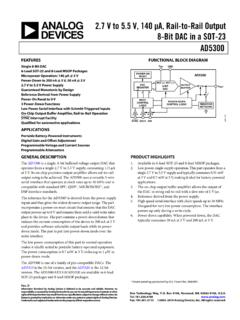
1 DAC5311-Q1.. SBAS470 JUNE 2009. V to V, 80 A, 8 BIT, LOW POWER, SINGLE CHANNEL, DIGITAL-TO-ANALOG CONVERTER. 1 FEATURES. RELATED.. 234 Qualified for Automotive Applications DEVICES 16-BIT 14-BIT 12-BIT 10-BIT 8-BIT. Relative Accuracy: LSB INL Pin and Function DAC8411 DAC8311 DAC7311 DAC6311 DAC5311. Micro-Power Operation: 80 A at V Compatible Power-Down: A at 5 V, A at V. AVDD GND. Wide Power Supply: V to V. Power-On Reset to Zero Scale Power-On Reset Straight Binary Data Format Low Power Serial Interface With REF(+). DAC output VOUT. Schmitt-Triggered Inputs: Up to 50 MHz Register 8-/10-/12-Bit Buffer DAC. On-Chip output Buffer Amplifier, Rail-to-Rail Operation SYNC Interrupt Facility Input Control Power-Down Resistor Tiny 6-Pin SC70 Package Logic Control Logic Network APPLICATIONS.
2 Portable, Battery-Powered instruments SYNC SCLK DIN. Process Control Digital Gain and Offset Adjustment Programmable Voltage and Current Sources DESCRIPTION. The DAC5311 is an 8-bit, low-power, SINGLE -channel, voltage output , digital-to-analog converters (DAC). It is monotonic by design and provides excellent linearity and minimizes undesired code-to-code transient voltages while offering an easy upgrade path within a pin-compatible family. The device uses a versatile, 3-wire serial interface that operates at clock rates of up to 50 MHz and is compatible with standard SPI , QSPI , MICROWIRE , and digital signal processor (DSP) interfaces. DAC5311 uses an external power supply as a reference voltage to set the output range.
3 The devices incorporate a power-on reset (POR) circuit that ensures the DAC output powers up at 0 V and remains there until a valid write to the device occurs. It contains a power-down feature, accessed over the serial interface, that reduces current consumption of the device to A at V in power-down mode. The low power consumption of this part in normal operation makes it ideally suited for portable battery-operated equipment. The power consumption is mW at 5 V, reducing to W in power-down mode. DAC5311 is pin-compatible with the DAC8311 and DAC8411, offering an easy upgrade path from 8-bit resolution to 14- and 16-bit resolution. The device is available in a small 6-pin SC70 package.
4 This package offers a flexible solution over the automotive temperature range of 40 C to 85 C. 1. Please be aware that an important notice concerning availability, standard warranty, and use in critical applications of Texas Instruments semiconductor products and disclaimers thereto appears at the end of this data sheet. 2 SPI, QSPI are trademarks of Motorola, Inc. 3 MICROWIRE is a trademark of National Semiconductor Corporation. 4 All other trademarks are the property of their respective owners. PRODUCTION DATA information is current as of publication date. Copyright 2009, Texas Instruments Incorporated Products conform to specifications per the terms of the Texas Instruments standard warranty.
5 Production processing does not necessarily include testing of all parameters. DAC5311-Q1. SBAS470 JUNE 2009 .. This integrated circuit can be damaged by ESD. Texas Instruments recommends that all integrated circuits be handled with appropriate precautions. Failure to observe proper handling and installation procedures can cause damage. ESD damage can range from subtle performance degradation to complete device failure. Precision integrated circuits may be more susceptible to damage because very small parametric changes could cause the device not to meet its published specifications. ORDERING INFORMATION (1). MAXIMUM MAXIMUM. RELATIVE DIFFERENTIAL ORDERABLE PART PACKAGE.
6 TA PACKAGE (2). ACCURACY NONLINEARITY NUMBER MARKING. (LSB) (LSB). 40 C to 85 C SC70-6 DCK Reel of 3000 DAC5311 IDCKRQ1 OCZ. (1) For the most current package and ordering information, see the Package Option Addendum at the end of this document, or see the TI. web site at (2) Package drawings, thermal data, and symbolization are available at ABSOLUTE MAXIMUM RATINGS (1). AVDD to GND V to 6 V. Digital input voltage to GND V to AVDD + V. AVOUT to GND V to AVDD + V. Operating temperature range 40 C to 85 C. Storage temperature range 65 C to 150 C. Junction temperature (TJ max) 150 C. Power dissipation (TJ max TA)/ JA W. JA thermal impedance 250 C/W. (1) Stresses above those listed under Absolute Maximum Ratings may cause permanent damage to the device.
7 Exposure to absolute maximum conditions for extended periods may affect device reliability. 2 Submit Documentation Feedback Copyright 2009, Texas Instruments Incorporated Product Folder Link(s): DAC5311-Q1. DAC5311-Q1.. SBAS470 JUNE 2009. ELECTRICAL CHARACTERISTICS. At AVDD = V to V, RL = 2 k to GND, CL = 200 pF to GND (unless otherwise noted). PARAMETER TEST CONDITIONS MIN TYP MAX UNIT. STATIC PERFORMANCE (1). Resolution 8 Bits Relative accuracy Measured by the line passing through codes 3 and 252 LSB. Differential nonlinearity LSB. Offset error Measured by the line passing through two codes (2) 4 mV. Offset error drift 3 V/ C. Zero code error All zeros loaded to the DAC register mV.
8 Full-scale error All ones loaded to DAC register % of FSR. Gain error % of FSR. AVDD = 5 V ppm of Gain temperature coefficient AVDD = V FSR/ C. output CHARACTERISTICS (3). output voltage range 0 AVDD V. RL = 2 k , CL = 200 pF, AVDD = 5 V, 1/4 scale to 3/4. 6 10 s output voltage settling time scale RL = 2 M , CL = 470 pF 12 s Slew rate V/ s RL = 470 pF. Capacitive load stability RL = 2 k 1000 pF. Code change glitch impulse 1-LSB change around major carry nV-s Digital feed through nV-s Power-on glitch impulse RL = 2 k , CL = 200 pF, AVDD = 5 V 17 mV. DC output impedance . AVDD = 5 V 50 mA. Short-circuit current AVDD = 3 V 20 mA. Power-up time Coming out of power-down mode 50 s AC PERFORMANCE.
9 SNR 81 dB. THD TA= 25 C, BW = 20 kHz, 12-bit level, AVDD = 5 V, 65 dB. fOUT = 1 kHz, 1st 19 harmonics removed for SNR. SFDR calculation 65 dB. SINAD 65 dB. TA= 25 C, at zero-scale input, fOUT = 1 kHz, AVDD = 5 V 17 nV/ Hz DAC output noise density (4). TA= 25 C, at mid-code input, fOUT = 1 kHz, AVDD = 5 V 110 nV/ Hz DAC output noise (5) TA= 25 C, at mid-code input, Hz to 10 Hz, AVDD = 5 V 3 VPP. (1) Linearity calculated using a reduced code range of 3 to 252, output unloaded. (2) Straight line passing through codes 3 and 252, output unloaded. (3) Specified by design and characterization, not production tested. (4) For more details, see Figure 16. (5) For more details, see Figure 17.
10 Copyright 2009, Texas Instruments Incorporated Submit Documentation Feedback 3. Product Folder Link(s): DAC5311-Q1. DAC5311-Q1. SBAS470 JUNE 2009 .. ELECTRICAL CHARACTERISTICS (continued). At AVDD = V to V, RL = 2 k to GND, CL = 200 pF to GND (unless otherwise noted). PARAMETER TEST CONDITIONS MIN TYP MAX UNIT. LOGIC INPUTS (6). Input current 1 A. AVDD = 5 V V. VINL, input low voltage AVDD = V V. AVDD = 5 V V. VINH, input high voltage AVDD = V V. Pin capacitance 3 pF. POWER REQUIREMENTS. AVDD V. AVDD = V to V 110 160. VINH = AVDD and VINL =. Normal mode AVDD = V to V 95 150 A. GND, at midscale code (7). AVDD = V to V 80 140. IDD. AVDD = V to V VINH = AVDD and VINL =.