Transcription of 14-Bit, 80 MSPS/155 MSPS, 1.8 V Dual Serial Output Analog …
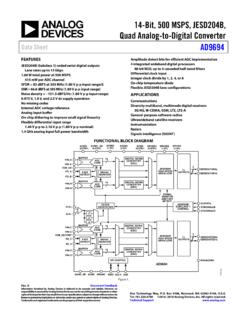
1 14-Bit, 80 MSPS/155 MSPS, V Dual Serial Output Analog -to- digital converter (ADC). Data Sheet AD9644. FEATURES FUNCTIONAL BLOCK DIAGRAM. AVDD AGND DRVDD DRGND. JESD204A coded Serial digital outputs SNR = dBFS at 70 MHz and 80 MSPS. AD9644 DOUT+A. CODING, SERIALIZER AND. SNR = dBFS at 70 MHz and 155 MSPS. JESD204A 8-BIT/10-BIT. VIN+A 14 DOUT A. PIPELINE. SFDR = 92 dBc at 70 MHz and 80 MSPS 14-BIT ADC. CML DRIVERS. VIN A DSYNC+A. SFDR = 92 dBc at 70 MHz and 155 MSPS VCMA DSYNC A. Low power: 423 mW at 80 MSPS, 567 mW at 155 MSPS. DOUT+B. V supply operation VIN+B PIPELINE 14 DOUT B. Integer 1-to-8 input clock divider 14-BIT ADC. VIN B DSYNC+B. IF sampling frequencies to 250 MHz VCMB DSYNC B. dBFS/Hz input noise at 180 MHz and 80 MSPS REFERENCE. PLL. dBFS/Hz input noise at 180 MHz and 155 MSPS. Programmable internal ADC voltage reference Flexible Analog input range: V p-p to V p-p PDWN Serial PORT 1 TO 8.
2 (SPI) CLOCK. ADC clock duty cycle stabilizer DIVIDER. Serial port control 09180-001. User-configurable, built-in self-test (BIST) capability SCLK SDIO CSB CLK+ CLK SYNC. Energy-saving power-down modes Figure 1. 48-Lead 7 mm 7 mm LFCSP. APPLICATIONS. Communications PRODUCT HIGHLIGHTS. Diversity radio systems 1. An on-chip PLL allows users to provide a single ADC. Multimode digital receivers (3G and 4G) sampling clock; the PLL multiplies the ADC sampling GSM, EDGE, W-CDMA, LTE, clock to produce the corresponding JESD204A data rate CDMA2000, WiMAX, TD-SCDMA clock. I/Q demodulation systems 2. The configurable JESD204A Output block supports up to Smart antenna systems Gbps per channel data rate when using a dedicated General-purpose software radios data link per ADC or Gbps data rate when using a Broadband data applications single shared data link for both ADCs. Ultrasound equipment 3.
3 Proprietary differential input that maintains excellent SNR. performance for input frequencies up to 250 MHz. 4. Operation from a single V power supply. 5. Standard Serial port interface (SPI) that supports various product features and functions, such as data formatting (offset binary, twos complement, or gray coding), controlling the clock DCS, power-down, test modes, voltage reference mode, and Serial Output configuration. Rev. D. Information furnished by Analog Devices is believed to be accurate and reliable. However, no responsibility is assumed by Analog Devices for its use, nor for any infringements of patents or other rights of third parties that may result from its use. Specifications subject to change without notice. One Technology Way, Box 9106, Norwood, MA 02062-9106, No license is granted by implication or otherwise under any patent or patent rights of Analog Tel: Devices.
4 Trademarks and registered trademarks are the property of their respective owners. Fax: 2010 2020 Analog Devices, Inc. All rights reserved. AD9644 Data Sheet TABLE OF CONTENTS. Features .. 1 Voltage Reference .. 22. Applications .. 1 Clock Input Considerations .. 22. Functional Block Diagram .. 1 Channel/Chip Synchronization .. 24. Product Highlights .. 1 Power Dissipation and Standby Mode .. 24. Revision History .. 2 digital Outputs .. 24. General Description .. 3 Built-In Self-Test (BIST) and Output Test .. 29. Specifications .. 4 Built-In Self-Test (BIST) .. 29. ADC DC Specifications .. 4 Output Test Modes .. 29. ADC AC Specifications .. 5 Serial Port Interface (SPI) .. 31. digital Specifications .. 6 Configuration Using the SPI .. 31. Switching Specifications .. 8 Hardware Interface .. 32. Timing Specifications .. 9 SPI Accessible Features .. 32. Absolute Maximum Ratings.
5 10 Memory Map .. 33. Thermal Characteristics .. 10 Reading the Memory Map Register Table .. 33. ESD 10 Memory Map Register Table .. 34. Pin Configuration and Function Descriptions .. 11 Memory Map Register Descriptions .. 38. Typical Performance Characteristics .. 13 Applications Information .. 42. Equivalent Circuits .. 19 Design Guidelines .. 42. Theory of Operation .. 20 Outline Dimensions .. 43. ADC Architecture .. 20 Ordering Guide .. 43. Analog Input Considerations .. 20. REVISION HISTORY. 9/2020 Rev. C to Rev. D 4/2011 Rev. 0 to Rev. A. Changed CP-48-8 to CP-48-9 .. Throughout Added Model -155 .. Throughout Updated Outline Dimensions .. 43 Changes to Features Section and Figure 1 ..1. Changes to Ordering Guide .. 43 Changes to General Description Section ..3. Changes to Table 1 ..4. 1/2012 Rev. B to Rev. C Changes to Table 2 ..5. Change to General Description Section.
6 3 Changes to Table 4 ..8. Additions to TPC Introductory Statement .. 13. 6/2011 Rev. A to Rev. B Changes to Speed Grade ID Bits in Table 17 .. 31. Added Figure 23 to Figure 40; Renumbered Sequentially .. 16 Changes to Ordering Guide .. 40. Changes to Clock Input Considerations Section .. 22. Added Figure 61 .. 24 6/2010 Revision 0: Initial Version Changes to digital Outputs and Timing Section .. 27. Added Figure 69 .. 28. Changes to Output Test Modes Section .. 29. Changes to SPI Accessible Features Section .. 32. Rev. D | Page 2 of 44. Data Sheet AD9644. GENERAL DESCRIPTION. The AD9644 is a dual, 14-bit, Analog -to- digital converter (ADC) By default, the ADC Output data is routed directly to the two with a high speed Serial Output interface and sampling speeds external JESD204A Serial Output ports. These outputs are at CML. of either 80 MSPS or 155 MSPS. voltage levels. Two modes are supported such that Output The AD9644 is designed to support communications appli- coded data is either sent through one data link or two.
7 (L = 1; F. cations where high performance, combined with low cost, small = 4 or size, and versatility, is desired. The JESD204A high speed Serial L = 2; F = 2). Independent synchronization inputs (DSYNC). interface reduces board routing requirements and lowers pin count are provided for each channel. requirements for the receiving device. Flexible power-down options allow significant power savings, The dual ADC core features a multistage, differential pipelined when desired. architecture with integrated Output error correction logic. Each Programming for setup and control is accomplished using a 3-wire ADC features wide bandwidth differential sample-and-hold SPI-compatible Serial interface. Analog input amplifiers that support a variety of user-selectable The AD9644 is available in a 48-lead LFCSP and is specified over input ranges. An integrated voltage reference eases design consid- the industrial temperature range of 40 C to +85 C.
8 Erations. A duty cycle stabilizer is provided to compensate for variations in the ADC clock duty cycle, allowing the converters This product is protected by a patent. to maintain excellent performance. Rev. D | Page 3 of 44. AD9644 Data Sheet SPECIFICATIONS. ADC DC SPECIFICATIONS. AVDD = V, DRVDD = V, maximum sample rate, V p-p differential input, VIN = dBFS differential input, DCS enabled, unless otherwise noted. Table 1. AD9644-80 AD9644-155. Parameter Temperature Min Typ Max Min Typ Max Unit RESOLUTION Full 14 14 Bits ACCURACY. No Missing Codes Full Guaranteed Guaranteed Offset Error Full 2 10 11 mV. Gain Error Full 7 +1 6 +4 % FSR. Differential Nonlinearity (DNL)1 Full LSB. 25 C LSB. Integral Nonlinearity (INL)1 Full LSB. 25 C LSB. MATCHING CHARACTERISTIC. Offset Error Full 7 + +10 6 + +9 mV. Gain Error Full + + + +5 % FSR. TEMPERATURE DRIFT. Offset Error Full 2 2 ppm/ C.
9 Gain Error Full 35 144 ppm/ C. INPUT REFERRED NOISE 25 C LSB rms Analog INPUT. Input Span Full V p-p Input Capacitance2 Full 7 5 pF. Input Resistance Full 20 20 k . VCM Output LEVEL Full V. POWER SUPPLIES. Supply Voltage AVDD Full V. DRVDD Full V. Supply Current IAVDD1 Full 175 190 226 242 mA. IDRVDD1 Full 60 67 89 97 mA. POWER CONSUMPTION. Sine Wave Input1 Full 423 460 567 610 mW. Standby Power3 Full 85 168 mW. Power-Down Power Full 15 27 18 27 mW. 1. Measured with a low input frequency, full-scale sine wave. 2. Input capacitance refers to the effective capacitance between one differential input pin and AGND. 3. Standby power is measured with a dc input and with the CLK pins inactive (set to AVDD or AGND). Rev. D | Page 4 of 44. Data Sheet AD9644. ADC AC SPECIFICATIONS. AVDD = V, DRVDD = V, maximum sample rate, V p-p differential input, VIN = dBFS differential input, DCS enabled, unless otherwise noted.
10 Table 2. AD9644-80 AD9644-155. Parameter1 Temperature Min Typ Max Min Typ Max Unit SIGNAL-TO-NOISE-RATIO (SNR). fIN = 10 MHz 25 C dBFS. fIN = 70 MHz 25 C dBFS. fIN = 180 MHz 25 C dBFS. AD9644 BCPZ-80 Full dBFS. AD9644 CCPZ-80 Full dBFS. AD9644 BCPZ-155 Full dBFS. fIN = 220 MHz 25 C dBFS. SIGNAL-TO-NOISE AND DISTORTION (SINAD). fIN = 10 MHz 25 C dBFS. fIN = 70 MHz 25 C dBFS. fIN = 180 MHz 25 C dBFS. AD9644 BCPZ-80 Full dBFS. AD9644 CCPZ-80 Full dBFS. AD9644 BCPZ-155 Full dBFS. fIN = 220 MHz 25 C dBFS. EFFECTIVE NUMBER OF BITS (ENOB). fIN = 10 MHz 25 C Bits fIN = 70 MHz 25 C Bits fIN = 180 MHz 25 C Bits fIN = 220 MHz 25 C Bits WORST SECOND OR THIRD HARMONIC. fIN = 10 MHz 25 C 94 94 dBc fIN = 70 MHz 25 C 92 92 dBc fIN = 180 MHz 25 C 87 92 dBc AD9644 BCPZ-80 Full 80 dBc AD9644 CCPZ-80 Full 73 dBc AD9644 BCPZ-155 Full 80 dBc fIN = 220 MHz 25 C 85 90 dBc SPURIOUS-FREE DYNAMIC RANGE (SFDR).