Transcription of 16-Bit, 10 MSPS, PulSAR Differential ADC Data Sheet AD7626
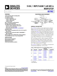
1 16 -Bit, 10 MSPS, PulSAR Differential ADC data Sheet AD7626 Rev. D Document Feedback Information furnished by analog devices is believed to be accurate and reliable. However, no responsibility is assumed by analog devices for its use, nor for any infringements of patents or other rights of third parties that may result from its use. Specifications subject to change without notice. No license is granted by implication or otherwise under any patent or patent rights of analog devices . Trademarks and registered trademarks are the property of their respective owners. One Technology Way, Box 9106, Norwood, MA 02062-9106, Tel: 2009 2016 analog devices , Inc. All rights reserved. Technical Support FEATURES Throughput: 10 MSPS SNR: dB 16-bit no missing codes INL: LSB DNL: LSB Power dissipation: 136 mW 32-lead LFCSP (5 mm 5 mm) SAR architecture No latency/pipeline delay 16-bit resolution with no missing codes Zero error: 1 LSB Differential input range: V Serial LVDS interface Self clocked mode Echoed clock mode LVDS or CMOS option for conversion control (CNV signal) Reference options Internal: V External ( V) buffered to V External: V APPLICATIONS Digital imaging systems Digital X-ray Digital MRI CCD and IR cameras High speed data acquisition High dynamic range telecommunications receivers Spectrum analysis Test equipment FUNCTIONAL BLOCK DIAGRAM AD7626 CLOCKLOGICSERIALLVDSIN IN+REFINREFVCMSAR 2 CNV+, CNV VIOD+, D DCO+, DCO CLK+, CLK GAPCAPDAC07648-001 Figure 1.
2 GENERAL DESCRIPTION The AD7626 is a 16-bit, 10 MSPS, charge redistribution successive approximation register (SAR) based architecture analog -to-digital converter (ADC). SAR architecture allows unmatched performance both in noise ( dB SNR) and in linearity ( LSB INL). The AD7626 contains a high speed, 16-bit sampling ADC, an internal conversion clock, and an internal buffered reference. On the CNV edge, it samples the voltage difference between the IN+ and IN pins. The voltages on these pins swing in opposite phase between 0 V and REF. The V reference voltage, REF, can be generated internally or applied externally. All converted results are available on a single low voltage Differential signaling (LV D S) self clocked or echoed clock serial interface, reducing external hardware connections. The AD7626 is housed in a 32-lead, 5 mm 5 mm LFCSP with operation specified from 40 C to +85 C. Table 1. Fast PulSAR ADC Selection Input Type Resolution (Bits) 1 MSPS to <2 MSPS 2 MSPS to 3 MSPS 5 MSPS to 6 MSPS 10 MSPS Differential (Ground Sense) 16 AD7653 AD7985 AD7667 AD7980 AD7983 True Bipolar 16 AD7671 Differential (Antiphase) 16 AD7677 AD7621 AD7625 AD7626 AD7623 AD7622 AD7961 Differential (Antiphase) 18 AD7643 AD7641 AD7960 AD7982 AD7986 AD7984 AD7626 data Sheet Rev.
3 D | Page 2 of 29 TABLE OF CONTENTS Features .. 1 Applications .. 1 Functional Block Diagram .. 1 General Description .. 1 Revision History .. 2 Specifications .. 3 Timing Specifications .. 6 Timing Diagrams .. 7 Absolute Maximum Ratings .. 8 Thermal Resistance .. 8 ESD Caution .. 8 Pin Configuration and Function Descriptions .. 9 Typical Performance Characteristics .. 11 Terminology .. 15 Theory of Operation .. 16 Circuit Information .. 16 Converter Information .. 16 Tr a n s fer Functions .. 17 analog 17 Typical Connection Diagram .. 18 Driving the 19 Voltage Reference Options .. 21 Power Supply .. 22 Digital Interface .. 23 Applications Information .. 25 Layout, Decoupling, and Grounding .. 25 Outline Dimensions .. 26 Ordering Guide .. 26 REVISION HISTORY 4/16 Rev. C to Rev. D Changes to Internal Reference Parameter, Table 2 .. 4 Added Acquisition Time Parameter, Table 3 .. 6 Change to Table 5 .. 8 Change to Figure 32 Caption and Figure 33 Caption.
4 19 10/15 Rev. B to Rev. C Changes to Table 1 .. 1 Added Aperture Delay Parameter and Current Drain Parameter, Ta b l e 2 .. 3 Changes to Ordering Guide .. 26 7/12 Rev. A to Rev. B Changed CP-32-2 Package to CP-32-7 Package .. Universal Changes to Figure 4 .. 8 Updated Outline Dimensions .. 25 Changes to Ordering Guide .. 25 1/10 Rev. 0 to Rev. A Changes to Description of Pin 5 and Pin 6, Table 6 .. 8 Changes to Power-Up Section .. 21 9/09 Revision 0: Initial Version data Sheet AD7626 Rev. D | Page 3 of 29 SPECIFICATIONS VDD1 = 5 V; VDD2 = V; VIO = V; REF = V; all specifications TMIN to TMAX, unless otherwise noted. Table 2. Parameter Test Conditions/Comments Min Typ Max Unit RESOLUTION 16 Bits analog INPUT Voltage Range VIN+ VIN VREF +VREF V Operating Input Voltage VIN+, VIN to AGND VREF + V Common-Mode Input Range VREF/2 VREF/2 VREF/2 + V CMRR fIN = 1 MHz 68 dB Input Current Midscale input 168 A THROUGHPUT Complete Cycle 100 ns Throughput Rate 10 MSPS DC ACCURACY Integral Linearity Error + LSB No Missing Codes 16 Bits Differential Linearity Error + LSB Transition Noise LSB Zero Error, TMIN to TMAX 6 1 +6 LSB Zero Error Drift ppm/ C Gain Error, TMIN to TMAX 8 20 LSB Gain Error Drift ppm/ C Power Supply Sensitivity1 VDD1 = 5 V 5% LSB VDD2 = V 5% LSB AC ACCURACY fIN = 20 kHz.
5 DBFS Dynamic Range dB Signal-to-Noise Ratio 90 91 dB Spurious-Free Dynamic Range 105 dB Total Harmonic Distortion dB Signal-to-(Noise + Distortion) 91 dB fIN = 100 kHz, dBFS Signal-to-Noise Ratio dB Spurious-Free Dynamic Range dB Total Harmonic Distortion dB Signal-to-(Noise + Distortion) 91 dB fIN = MHz, 1 dBFS Signal-to-Noise Ratio dBFS Spurious-Free Dynamic Range 84 dB Total Harmonic Distortion 86 dB Signal-to-(Noise + Distortion) 85 dB fIN = MHz, 6 dBFS Signal-to-Noise Ratio 89 dBFS Spurious-Free Dynamic Range 84 dB Total Harmonic Distortion 93 dB Signal-to-(Noise + Distortion) 88 dB 3 dB Input Bandwidth 95 MHz Aperture Delay ns Aperture Jitter ps rms AD7626 data Sheet Rev. D | Page 4 of 29 Parameter Test Conditions/Comments Min Typ Max Unit INTERNAL REFERENCE Output Voltage REFIN at 25 C V Temperature Drift 40 C to +85 C 15 ppm/ C REFERENCE BUFFER REFIN Input Voltage Range V REF Output Voltage Range REF at 25 C, EN0 = EN1 = 1 V Line Regulation VDD1 5%, VDD2 5% 5 mV EXTERNAL REFERENCE Voltage Range REF V Current Drain 10 MSPS 570 A VCM PIN VCM Output REF/2 VCM Error + V Output Impedance 5 k LVDS I/O (ANSI-644)
6 data Format Serial LVDS twos complement Differential Output Voltage, VOD RL = 100 245 290 454 mV Common-Mode Output Voltage, VOCM RL = 100 9802 1130 1375 mV Differential Input Voltage, VID 100 650 mV Common-Mode Input Voltage, VICM 800 1575 mV POWER SUPPLIES Specified Performance VDD1 5 V VDD2 V VIO V Operating Currents Static Not Converting VDD1 mA VDD2 mA VIO mA With Internal Reference 10 MSPS throughput VDD1 mA VDD2 mA VIO Echoed clock mode mA With External Reference 10 MSPS throughput VDD1 mA VDD2 23 28 mA VIO Echoed clock mode mA Power-Down EN0 = 0, EN1 = 0 VDD1 4 A VDD2 10 A VIO 1 5 A Power Dissipation3 Static Not Converting 88 107 mW With Internal Reference 10 MSPS throughput 150 170 mW With External Reference 10 MSPS throughput 136 160 mW Power-Down 8 58 W Energy per Conversion 10 MSPS throughput nJ/sample data Sheet AD7626 Rev.
7 D | Page 5 of 29 Parameter Test Conditions/Comments Min Typ Max Unit TEMPERATURE RANGE Specified Performance TMIN to TMAX 40 +85 C 1 Using an external reference. 2 The ANSI-644 LVDS I/O specification has a minimum output common mode (VOCM) of 1125 mV. 3 Power dissipation is for the AD7626 device only. In self clocked interface mode, mW is dissipated in the 100 terminator. In echoed clock interface mode, mW is dissipated in two 100 terminators. AD7626 data Sheet Rev. D | Page 6 of 29 TIMING SPECIFICATIONS VDD1 = 5 V; VDD2 = V; VIO = V to V; REF = V; all specifications TMIN to TMAX, unless otherwise noted. Table 3. Parameter Symbol Min Typ Max Unit Time Between Conversions1 tCYC 100 10,000 ns Acquisition Time tACQ 40 ns CNV High Time tCNVH 10 40 ns CNV to D (MSB) Ready tMSB 100 ns CNV to Last CLK (LSB) Delay tCLKL 72 ns CLK Period2 tCLK 4 (tCYC tMSB + tCLKL)/n ns CLK Frequency fCLK 250 300 MHz CLK to DCO Delay (Echoed Clock Mode) tDCO 0 4 7 ns DCO to D Delay (Echoed Clock Mode) tD 0 1 ns CLK to D Delay tCLKD 0 4 7 ns 1 The maximum time between conversions is 10,000 ns.
8 If CNV is left idle for a time greater than the maximum value of tCYC, the subsequent conversion result is invalid. 2 For the maximum CLK period, the window available to read data is tCYC tMSB + tCLKL. Divide this time by the number of bits (n) to be read giving the maximum CLK frequency that can be used for a given conversion CNV frequency. In echoed clock interface mode, n = 16; in self clocked interface mode, n = 18. data Sheet AD7626 Rev. D | Page 7 of 29 TIMING DIAGRAMS CLK+tCYC1615 CNV+116152123tCNVHtCLKLDCO+1615116152123 D+SAMPLE NSAMPLE N + 1D D15ND14ND1 NCLK CNV DCO D0N 1 ACQUISITIONACQUISITIONACQUISITIONtDCOtDt CLK0tMSBD1N 1D15N + 1D14N + 1D0N0D13N + 1tCLKD07648-003 Figure 2. Echoed Clock Interface Mode Timing Diagram CLK+1817142123tCLKLD+D CLK D0N 1D1N 1 ACQUISITIONACQUISITIONACQUISITIONtCLKDtC LKtMSB18173D15ND14ND1N001D0ND15N + 1001tCYCCNV+tCNVHSAMPLE NSAMPLE N + 1 CNV 07648-004 Figure 3. Self Clocked Interface Mode Timing Diagram AD7626 data Sheet Rev.
9 D | Page 8 of 29 ABSOLUTE MAXIMUM RATINGS Table 4. Parameter Rating analog Inputs/Outputs IN+, IN to GND1 V to REF + V or 130 mA REF2 to GND V to +6 V VCM, CAP2 to GND V to +6 V CAP1, REFIN to GND V to + V Supply Voltage VDD1 V to +6 V VDD2, VIO V to +3 V Digital Inputs to GND V to VIO + V Digital Outputs to GND V to VIO + V Input Current to Any Pin Except Supplies3 10 mA Operating Temperature Range (Commercial) 40 C to +85 C Storage Temperature Range 65 C to +150 C Junction Temperature 150 C ESD 1 kV 1 See the analog Inputs section. 2 Keep CNV low for any external REF voltage > V applied to the REF pin. 3 Transient currents of up to 100 mA do not cause SCR latch-up. Stresses at or above those listed under Absolute Maximum Ratings may cause permanent damage to the product. This is a stress rating only; functional operation of the product at these or any other conditions above those indicated in the operational section of this specification is not implied.
10 Operation beyond the maximum operating conditions for extended periods may affect product reliability. THERMAL RESISTANCE JA is specified for the worst case conditions, that is, a device soldered in a circuit board for surface-mount packages. Table 5. Thermal Resistance Package Type JA JC Unit 32-Lead LFCSP_WQ 40 4 C/W ESD CAUTION data Sheet AD7626 Rev. D | Page 9 of 29 PIN CONFIGURATION AND FUNCTION DESCRIPTIONS 07648-002 NOTES1. CONNECT THE EXPOSED PAD TO THE GROUND PLANE OF THE PCB USING MULTIPLE GNDIN+IN VCMVDD1 VDD1 VDD2 CLK+CNV+D D+VIOGNDDCO DCO+CLK REFGNDREFREFCAP2 GNDCAP2 CAP2123456782423222120191817910111213141 5163231302928272625AD7626 TOP VIEW(Not to Scale) Figure 4. Pin Configuration Table 6. Pin Function Descriptions Pin No. Mnemonic Type1 Description 1 VDD1 P analog 5 V Supply. Decouple the 5 V supply with a 100 nF capacitor. 2 VDD2 P analog V Supply. Decouple this pin with a 100 nF capacitor.