Transcription of 16-Bit, 100 kSPS, Single-Ended PulSAR ADC in …
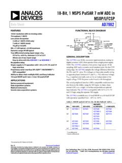
1 16-Bit, 100 ksps , Single-Ended PulSAR ADC in msop /QFN. data sheet AD7683. FEATURES APPLICATION DIAGRAM. TO VDD TO 16-bit resolution with no missing codes Throughput: 100 ksps . INL: 1 LSB typical, 3 LSB maximum REF VDD. 0V TO VREF. Pseudo differential analog input range +IN DCLOCK. 0 V to VREF with VREF up to VDD IN AD7683 DOUT. 3-WIRE SPI. INTERFACE. Single-supply operation: V to V GND. CS. 04301-001. Serial interface SPI/QSPI/MICROWIRE/DSP compatible Power dissipation: 4 mW @ 5 V, mW @ V, Figure 1. 150 W @ V/10 ksps . Standby current: 1 nA. 8-lead packages: msop . Table 1. msop , QFN (LFCSP)/SOT-23, 14-/16-/18-Bit 3 mm 3 mm QFN (LFCSP) (SOT-23 size) PulSAR ADC. 400 ksps . Improved second source to ADS8320 and ADS8325. 100 250 to 1000 ADC. Type ksps ksps 500 ksps ksps Driver 18-Bit True AD7691 AD7690 AD7982 ADA4941-1. APPLICATIONS Differential AD7984 ADA4841-1.
2 Battery-powered equipment 16-Bit True AD7684 AD7687 AD7688 ADA4941-1. data acquisition Differential AD7693 ADA4841-1. Instrumentation 16-Bit AD7680 AD7685 AD7686 AD7980 ADA4841-1. Pseudo AD7683 AD7694. Medical instruments Differential Process control 14-Bit AD7940 AD7942 AD7946 ADA4841-1. Pseudo Differential GENERAL DESCRIPTION. The AD7683 is a 16-bit, charge redistribution, successive analog input, +IN, between 0 V to REF with respect to a ground approximation, PulSAR analog -to-digital converter (ADC) sense, IN. The reference voltage, REF, is applied externally and that operates from a single power supply, VDD, between V can be set up to the supply voltage. Its power scales linearly with and V. It contains a low power, high speed, 16-bit sampling throughput. ADC with no missing codes (B grade), an internal conversion The AD7683 is housed in an 8-lead msop or an 8-lead QFN.
3 Clock, and a serial, SPI-compatible interface port. The part also (LFCSP) package, with an operating temperature specified from contains a low noise, wide bandwidth, short aperture delay, 40 C to +85 C. track-and-hold circuit. On the CS falling edge, it samples an Rev. B Document Feedback Information furnished by analog devices is believed to be accurate and reliable. However, no responsibility is assumed by analog devices for its use, nor for any infringements of patents or other rights of third parties that may result from its use. Specifications subject to change without notice. No One Technology Way, Box 9106, Norwood, MA 02062-9106, license is granted by implication or otherwise under any patent or patent rights of analog devices . Tel: 2004 2016 analog devices , Inc. All rights reserved. Trademarks and registered trademarks are the property of their respective owners.
4 Technical Support AD7683 data sheet TABLE OF CONTENTS. Features .. 1 Circuit 12 Applications .. 1 Converter 12 Application Diagram .. 1 Transfer Functions .. 12 General Description .. 1 Typical Connection Diagram .. 13 Revision History .. 2 analog Input .. 13 3 Driver Amplifier Choice .. 13 Timing Specifications .. 5 Voltage Reference Input .. 14 Absolute Maximum 6 Power 14 Thermal Resistance .. 6 Digital Interface .. 14 ESD Caution .. 6 Layout .. 14 Pin Configurations and Function Descriptions .. 7 Evaluating the AD7683 Performance .. 14 Terminology .. 8 Outline Dimensions .. 15 Typical Performance Characteristics .. 9 Ordering Guide .. 16 Applications Information .. 12 REVISION HISTORY. 2/16 Rev. A to Rev. B. Changes to Table 1 .. 1. Added Figure 7 and Table 9; Renumbered Sequentially .. 7. Changes to Table 10 .. 13. Changes to Digital Interface 14.
5 Updated Outline Dimensions .. 16. Changes to Ordering Guide .. 16. 2/08 Rev. 0 to Rev. A. Change to Title .. 1. Moved Figure 3, Figure 4, and Figure 5 .. 5. Changes to Figure 4 .. 5. Moved Figure 17 and Figure 18 .. 11. Changes to Figure 22 .. 13. Updated Outline Dimensions .. 15. Changes to Ordering Guide .. 16. 9/04 Initial Version: Revision 0. Rev. B | Page 2 of 16. data sheet AD7683. SPECIFICATIONS. VDD = V to V; VREF = VDD; TA = 40 C to +85 C, unless otherwise noted. Table 2. AD7683 All Grades Parameter Conditions Min Typ Max Unit RESOLUTION 16 Bits analog INPUT. Voltage Range +IN ( IN) 0 VREF V. Absolute Input Voltage +IN VDD + V. IN V. analog Input CMRR fIN = 100 kHz 65 dB. Leakage Current at 25 C Acquisition phase 1 nA. Input Impedance See the analog Input section THROUGHPUT SPEED. Complete Cycle 10 s Throughput Rate 0 100 ksps .
6 DCLOCK Frequency 0 MHz REFERENCE. Voltage Range VDD + V. Load Current 100 ksps , V+IN V IN = VREF/2 = V 50 A. DIGITAL INPUTS. Logic Levels VIL VDD V. VIH VDD VDD + V. IIL 1 +1 A. IIH 1 +1 A. Input Capacitance 5 pF. DIGITAL OUTPUTS. data Format Serial, 16 bits straight binary VOH ISOURCE = 500 A VDD V. VOL ISINK = +500 A V. POWER SUPPLIES. VDD Specified performance V. VDD Range1 V. Operating Current 100 ksps throughput VDD VDD = 5 V 800 A. VDD = V 560 A. Standby Current2, 3 VDD = 5 V, 25 C 1 50 nA. Power Dissipation VDD = 5 V 4 6 mW. VDD = V mW. VDD = V, 10 ksps throughput2 150 W. TEMPERATURE RANGE. Specified Performance TMIN to TMAX 40 +85 C. 1. See the Typical Performance Characteristics section for more information. 2. With all digital inputs forced to VDD or GND, as required. 3. During acquisition phase. Rev. B | Page 3 of 16. AD7683 data sheet VDD = 5 V; VREF = VDD; TA = 40 C to +85 C, unless otherwise noted.
7 Table 3. A Grade B Grade Parameter Conditions Min Typ Max Min Typ Max Unit ACCURACY. No Missing Codes 15 16 Bits Integral Linearity Error 6 3 +6 3 1 +3 LSB. Transition Noise LSB. Gain Error1, TMIN to TMAX 2 24 2 15 LSB. Gain Error Temperature Drift ppm/ C. Offset Error1, TMIN to TMAX mV. Offset Temperature Drift ppm/ C. Power Supply Sensitivity VDD = 5 V 5% LSB. AC ACCURACY. Signal-to-Noise fIN = 1 kHz 90 88 91 dB2. Spurious-Free Dynamic Range fIN = 1 kHz 100 108 dB. Total Harmonic Distortion fIN = 1 kHz 100 106 dB. Signal-to-(Noise + Distortion) fIN = 1 kHz 90 88 91 dB. Effective Number of Bits fIN = 1 kHz Bits 1. See the Terminology section. These specifications include full temperature range variation but do not include the error contribution from the external reference. 2. All specifications in dB are referred to a full-scale input, FS.
8 Tested with an input signal at dB below full scale, unless otherwise specified. VDD = V; VREF = ; TA = 40 C to +85 C, unless otherwise noted. Table 4. A Grade B Grade Parameter Conditions Min Typ Max Min Typ Max Unit ACCURACY. No Missing Codes 15 16 Bits Integral Linearity Error 6 3 +6 3 1 +3 LSB. Transition Noise LSB. Gain Error1, TMIN to TMAX 2 30 2 15 LSB. Gain Error Temperature Drift ppm/ C. Offset Error1, TMIN to TMAX mV. Offset Temperature Drift ppm/ C. Power Supply Sensitivity VDD = V 5% LSB. AC ACCURACY. Signal-to-Noise fIN = 1 kHz 85 86 dB2. Spurious-Free Dynamic Range fIN = 1 kHz 96 100 dB. Total Harmonic Distortion fIN = 1 kHz 94 98 dB. Signal-to-(Noise + Distortion) fIN = 1 kHz 85 86 dB. Effective Number of Bits fIN = 1 kHz 14 Bits 1. See the Terminology section. These specifications do include full temperature range variation but do not include the error contribution from the external reference.
9 2. All specifications in dB are referred to a full-scale input FS. Tested with an input signal at dB below full scale, unless otherwise specified. Rev. B | Page 4 of 16. data sheet AD7683. TIMING SPECIFICATIONS. VDD = V to V; TA = 40 C to +85 C, unless otherwise noted. Table 5. Parameter Symbol Min Typ Max Unit Throughput Rate tCYC 100 kHz CS Falling to DCLOCK Low tCSD 0 s CS Falling to DCLOCK Rising tSUCS 20 ns DCLOCK Falling to data Remains Valid tHDO 5 16 ns CS Rising Edge to DOUT High Impedance tDIS 14 100 ns DCLOCK Falling to data Valid tEN 16 50 ns Acquisition Time tACQ 400 ns DOUT Fall Time tF 11 25 ns DOUT Rise Time tR 11 25 ns Timing and Circuit Diagrams tCYC. COMPLETE CYCLE. CS. tSUCS tACQ. POWER DOWN. DCLOCK 1 4 5. tCSD tEN tHDO tDIS. HIGH-Z HIGH-Z. DOUT 0 D15 D14 D13 D12 D11 D10 D9 D8 D7 D6 D5 D4 D3 D2 D1 D0 0. (MSB) (LSB).
10 NOTES. 04301-002. 1. A MINIMUM OF 22 CLOCK CYCLES ARE REQUIRED FOR 16-BIT CONVERSION. SHOWN ARE 24 CLOCK CYCLES. DOUT GOES LOW ON THE DCLOCK FALLING EDGE FOLLOWING THE LSB READING. Figure 2. Serial Interface Timing 500 A IOL. TO DOUT CL. 100pF. 04301-003. 500 A IOH. Figure 3. Load Circuit for Digital Interface Timing 2V. tEN tEN. 04301-004. 2V 2V. Figure 4. Voltage Reference Levels for Timing 90%. DOUT. 10%. 04301-006. tR tF. Figure 5. DOUT Rise and Fall Timing Rev. B | Page 5 of 16. AD7683 data sheet ABSOLUTE MAXIMUM RATINGS. Table 6. Stresses at or above those listed under Absolute Maximum Parameter Rating Ratings may cause permanent damage to the product. This is a analog Inputs stress rating only; functional operation of the product at these +IN1, IN1 GND V to VDD + V or or any other conditions above those indicated in the operational 130 mA.