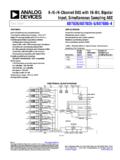
Transcription of 16-Channel DAS with 16-Bit, Bipolar Input, Dual ...
1 16 - channel DAS with 16-Bit, Bipolar input , dual simultaneous sampling ADC Data Sheet AD7616 Rev. 0 Document Feedback Information furnished by analog devices is believed to be accurate and reliable. However, no responsibility is assumed by analog devices for its use, nor for any infringements of patents or other rights of third parties that may result from its use. Specifications subject to change without notice. No license is granted by implication or otherwise under any patent or patent rights of analog devices . Trademarks and registered trademarks are the property of their respective owners.
2 One Technology Way, Box 9106, Norwood, MA 02062-9106, Tel: 2016 analog devices , Inc. All rights reserved. Technical Support FEATURES 16-Channel , dual , simultaneously sampled inputs Independently selectable channel input ranges True Bipolar : 10 V, 5 V, V Single 5 V analog supply and V to V VDRIVE supply Fully integrated data acquisition solution analog input clamp protection input buffer with 1 M analog input impedance First-order antialiasing analog filter On-chip accurate reference and reference buffer dual 16-bit successive approximation register (SAR) ADC Throughput rate: 2 1 MSPS Oversampling capability with digital filter Flexible sequencer with burst mode Flexible parallel/serial interface SPI/QSPI/MICROWIRE/DSP compatible Optional cyclic redundancy check (CRC) error checking Hardware/software configuration Performance 92 dB SNR at 500 kSPS (2 oversampling) dB SNR at 1 MSPS 103 dB THD 1 LSB INL (typical), LSB DNL (maximum) 8 kV ESD rating on analog input channels On-chip self detect function 80-lead LQFP package APPLICATIONS Power line monitoring Protective relays Multiphase motor control Instrumentation and control systems Data acquisition systems (DASs)
3 GENERAL DESCRIPTION The AD7616 is a 16-bit, DAS that supports dual simultaneous sampling of 16 channels. The AD7616 operates from a single 5 V supply and can accommodate 10 V, 5 V, and V true Bipolar input signals while sampling at throughput rates up to 1 MSPS per channel pair with dB SNR. Higher SNR performance can be achieved with the on-chip oversampling mode (92 dB for an oversampling ratio (OSR) of 2). The input clamp protection circuitry can tolerate voltages up to 21 V. T h e AD7616 has 1 M analog input impedance, regardless of sampling frequency. The single-supply operation, on-chip filtering, and high input impedance eliminate the need for driver op amps and external Bipolar supplies.
4 The device contains analog input clamp protection, a dual , 16-bit charge redistribution SAR analog -to-digital converter (ADC), a flexible digital filter, a V reference and reference buffer, and high speed serial and parallel interfaces. The AD7616 is serial peripheral interface (SPI)/QSPI /DSP/ MICROWIRE compatible FUNCTIONAL BLOCK DIAGRAM Figure 1. 13591-001 RFB1M 1M RFBFIRST-ORDER LPFRFB1M 1M RFBFIRST-ORDER LPFV0AV0 AGNDRFB1M 1M RFBV7AV7 AGNDV0BV0 BGNDV7BV7 BGND9:1 MUXBUSYCONVSTCONTROLINPUTSCLK MULTIFUNCTION PINS, SUCH AS DB15/OS2, ARE REFERRED TO BY A SINGLE FUNCTION OF THE PIN, FOR EXAMPLE, DB15, WHEN ONLY THAT FUNCTION IS RELEVANT.
5 REFER TO THE PIN CONFIGURATION AND FUNCTION DESCRIPTIONS SECTION FOR MORE :1 MUX16-BITSAR16-BITSAROS2 TO OS0 VDRIVEVCCALDO2:1 MUXHW_RNGSEL0, HW_RNGSEL1 CHSEL2 TO CHSEL0 SEQENFLEXIBLESEQUENCERBURSTRESETAGNDDGND DB15 TO DB0 SDOx/SDIPARALLELFIRST-ORDER LPFRFB1M 1M RFBFIRST-ORDER Data Sheet Rev. 0 | Page 2 of 50 TABLE OF CONTENTS Features .. 1 Applications .. 1 General Description .. 1 Functional Block Diagram .. 1 Revision History .. 2 Specifications .. 3 Timing Specifications .. 6 Parallel Mode Timing Specifications .. 8 Serial Mode Timing Specifications .. 9 Absolute Maximum Ratings .. 10 Thermal Resistance.
6 10 ESD Caution .. 10 Pin Configuration and Function Descriptions .. 11 Typical Performance Characteristics .. 15 Terminology .. 21 Theory of Operation .. 23 Converter 23 analog input .. 23 ADC Transfer Function .. 24 Internal/External Reference .. 24 Shutdown Mode .. 25 Digital Filter .. 25 Applications Information .. 26 Functionality Overview .. 26 Device Configuration .. 28 Operational Mode .. 28 Internal/External Reference .. 28 Digital Interface .. 28 Hardware Mode .. 28 Software Mode .. 29 Reset 29 Pin Function Overview .. 30 Digital Interface .. 31 channel Selection .. 31 Parallel Interface .. 32 Serial Interface.
7 33 35 Hardware Mode Sequencer .. 35 Software Mode Sequencer .. 35 Burst Sequencer .. 36 Diagnostics .. 38 Diagnostic Channels .. 38 Interface Self Test .. 38 CRC .. 38 Register Summary .. 40 Addressing Registers .. 41 Configuration Register .. 42 channel Register .. 43 input Range Registers .. 44 input Range Register 44 input Range Register 45 input Range Register B1 .. 46 input Range Register B2 .. 47 Sequencer Stack Registers .. 48 Status Register .. 49 Outline Dimensions .. 50 Ordering Guide .. 50 REVISION HISTORY 10/2016 Revision 0: Initial Version Data Sheet AD7616 Rev. 0 | Page 3 of 50 SPECIFICATIONS VREF = V external/internal, VCC = V to V, VDRIVE = V to V, fSAMPLE = 1 MSPS, TA = 40 C to +125 C, unless otherwise noted.
8 Table 1. Parameter Test Conditions/Comments Min Typ Max Unit DYNAMIC PERFORMANCE Signal-to-Noise Ratio (SNR)1, 2 89 dB 92 dB 93 dB88 dB 87 dB Signal-to-Noise-and-Distortion (SINAD)1 90 dB 89 dB 85 87 dB Dynamic Range 92 dB dB 88 dB Total Harmonic Distortion (THD)1 103 dB 100 dB fIN = 1 kHz sine wave unless otherwise noted No oversampling, 10 V range OSR = 2, 10 V range,3 fSAMPLE = 500 kSPS OSR = 4, 10 V range3No oversampling, 5 V range No oversampling, V range No oversampling, 10 V range No oversampling, 5 V range No oversampling, V range No oversampling, 10 V range No oversampling, 5 V range No oversampling, V range No oversampling, 10 V range No oversampling, 5 V range No oversampling, V range 97 dB Peak Harmonic or Spurious Noise1 103 dB Intermodulation Distortion (IMD)
9 1 fa = 1 kHz, fb = kHz Second-Order Terms 105 dB Third-Order Terms 113 dB channel to channel Isolation1fIN on unselected channels up to 5 kHz 106 dB analog input FILTER Full Power Bandwidth 3 dB, 10 V range 39 kHz 3 dB, 5 V range 33 kHz kHzPhase Delay3 10 V range s 5 V range5 s V sPhase Delay Drift3 10 V range ns/ CPhase Delay Matching ( dual )
10 simultaneous Pair)3 10 V range 100 ns 5 V ns V range ns DC ACCURACY Resolution No missing codes 16 Bits Differential Nonlinearity (DNL)1 LSB4 Integral Nonlinearity (INL)1 1 2 LSBT otal Unadjusted Error (TUE) 10 V range 6 LSB 5 V range 8 LSB V range 10 LSBP ositive Full-Scale Error5 External reference 10 V range 5 32 LSB 5 V range 4 LSB V range 2 LSB Internal reference 10 V range 5 LSBAD7616 Data Sheet Rev.
