Transcription of 2.7 V to 5.5 V, 140 μA, Rail-to-Rail Output 8-Bit DAC in a ...
1 V to V, 140 A, Rail-to-Rail Output 8-Bit DAC in a SOT-23 AD5300 Rev. D Information furnished by analog devices is believed to be accurate and reliable. However, no responsibility is assumed by analog devices for its use, nor for any infringements of patents or other rights of third parties that may result from its use. Specifications subject to change without notice. No license is granted by implication or otherwise under any patent or patent rights of analog devices . Trademarks and registered trademarks are the property of their respective owners.
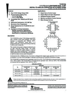
2 One Technology Way, Box 9106, Norwood, MA 02062-9106, : Fax: 2003 2010 analog devices , Inc. All rights reserved. FEATURES Single 8-Bit DAC 6-Lead SOT-23 and 8-Lead MSOP Packages Micropower Operation: 140 A @ 5 V Power-Down to 200 nA @ 5 V, 50 nA @ 3 V V to V Power Supply Guaranteed Monotonic by Design Reference Derived from Power Supply Power-On Reset to 0 V 3 Power-Down Functions Low Power Serial Interface with Schmitt-Triggered Inputs On-Chip Output Buffer Amplifier, Rail-to-Rail Operation SYNC Interrupt Facility Qualified for automotive applications APPLICATIONS Portable Battery-Powered Instruments Digital Gain and Offset Adjustment Programmable Voltage and Current Sources Programmable Attenuators FUNCTIONAL BLOCK DIAGRAM AD5300 GNDSYNC SCLK DINVDDVOUTOUTPUTBUFFER8-BITDACREF (+) REF ( )
3 POWER-ONRESETDACREGISTERINPUTCONTROLLOGI CPOWER-DOWNCONTROL LOGICRESISTORNETWORK00471-001 GENERAL DESCRIPTION The AD5300 is a single, 8-Bit buffered voltage Output DAC that operates from a single V to V supply, consuming 115 A at 3 V. Its on-chip precision Output amplifier allows Rail-to-Rail Output swing to be achieved. The AD5300 uses a versatile 3-wire serial interface that operates at clock rates up to 30 MHz and is compatible with standard SPI , QSPI , MICROWIRE , and DSP interface standards. The reference for the AD53001 is derived from the power supply inputs and thus gives the widest dynamic Output range.
4 The part incorporates a power-on reset circuit that ensures that the DAC Output powers up to 0 V and remains there until a valid write takes place to the device. The part contains a power-down feature that reduces the current consumption of the device to 200 nA at 5 V and provides software selectable Output loads while in power-down mode. The part is put into power-down mode over the serial interface. The low power consumption of this part in normal operation makes it ideally suited to portable battery-operated equipment. The power consumption is mW at 5 V, reducing to 1 W in power-down mode.
5 The AD5300 is one of a family of pin-compatible DACs. The AD5310 is the 10-bit version, and the AD5320 is the 12-bit version. The AD5300/AD5310/AD5320 are available in 6-lead SOT-23 packages and 8-lead MSOP packages. PRODUCT HIGHLIGHTS 1. Available in 6-lead SOT-23 and 8-lead MSOP packages. 2. Low power, single-supply operation. This part operates from a single V to V supply and typically consumes mW at 3 V and mW at 5 V, making it ideal for battery-powered applications. 3. The on-chip Output buffer amplifier allows the Output of the DAC to swing Rail-to-Rail with a slew rate of 1 V/ s.
6 4. Reference derived from the power supply. 5. High speed serial interface with clock speeds up to 30 MHz. Designed for very low power consumption. The interface powers up only during a write cycle. 6. Power-down capability. When powered down, the DAC typically consumes 50 nA at 3 V and 200 nA at 5 V. 1 Patent pending; protected by Patent No. 5684481. 2 REV. AD5300 SPECIFICATIONS(VDD = V to V; RL = 2 k to GND; CL = 500 pF to GND; all specificationsTMIN to TMAX, unless otherwise noted.)B Version1 ParameterMinTypMaxUnitConditions/Comment sSTATIC PERFORMANCE2 Resolution8 BitsRelative Accuracy 1 LSBSee Figure Nonlinearity Monotonic by Design.
7 See Figure Error+ + Zeros Loaded to DAC Register. See Figure Error Ones Loaded to DAC Register. See Figure Error of FSRZero-Code Error Drift 20 V/ CGain Temperature Coefficient 5ppm of FSR/ COUTPUT CHARACTERISTICS3 Output Voltage Range0 VDDVO utput Voltage Settling Time46 s1/4 Scale to 3/4 Scale Change (40 Hex to C0 Hex).RL = 2 k ; 0 pF < CL < 500 pF. See Figure Rate1V/ sCapacitive Load Stability470pFRL = .1000pFRL = 2 k .Digital-to- analog Glitch Impulse20nV-s1 LSB Change Around Major Carry. See Figure Output Impedance1 Short-Circuit Current50mAVDD = 5 = 3 sComing Out of Power-Down Mode.
8 VDD = 5 sComing Out of Power-Down Mode. VDD = 3 INPUTS3 Input Current 1 AVINL, Input Low = 5 , Input Low = 3 , Input High = 5 , Input High = 3 Capacitance3pFPOWER (Normal Mode)DAC Active and Excluding Load = V to V140250 AVIH = VDD and VIL = = V to V115200 AVIH = VDD and VIL = (All Power-Down Modes)VDD = V to AVIH = VDD and VIL = = V to AVIH = VDD and VIL = EFFICIENCYIOUT/IDD93%ILOAD = 2 mA. VDD = 5 range as follows: B Version: 40 C to +105 calculated using a reduced code range of 4 to 251.
9 Output by design and characterization, not production subject to change without 3 REV. TIMING CHARACTERISTICS1, 2 Limit at TMIN, TMAXP arameterVDD = V to VVDD = V to VUnitConditions/Commentst135033ns minSCLK Cycle Timet21313ns minSCLK High minSCLK Low Timet41313ns minSYNC to SCLK Falling Edge Setup Timet555ns minData Setup minData Hold Timet700ns minSCLK Falling Edge to SYNC Rising Edget85033ns minMinimum SYNC High TimeNOTES1 All input signals are specified with tr = tf = 5 ns (10% to 90% of VDD) and timed from a voltage level of (VIL + VIH)
10 Figure SCLK frequency is 30 MHz at VDD = V to V and 20 MHz at VDD = V to subject to change without t1 Figure 1. Serial Write Operation(VDD = V to V; all specifications TMIN to TMAX, unless otherwise noted.)ABSOLUTE MAXIMUM RATINGS*(TA = 25 C, unless otherwise noted.)VDD to GND .. V to +7 VDigital Input Voltage to GND .. V to VDD + VVOUT to GND .. V to VDD + VOperating Temperature RangeIndustrial (B Version) .. 40 C to +105 CStorage Temperature Range .. 65 C to +150 CJunction Temperature (TJ max).