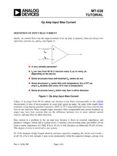
Transcription of 2.7V to 5.5V Single Supply CMOS Op Amp
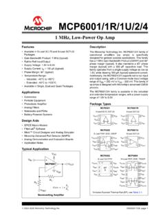
1 2007 Microchip Technology 1 MCP601/1R/2/3/4 Features Single - Supply : to Rail-to-Rail Output Input Range Includes Ground Gain Bandwidth Product: MHz (typical) Unity-Gain Stable Low Quiescent Current: 230 A/amplifier (typical) Chip Select (CS): MCP603 only Temperature Ranges:- Industrial: -40 C to +85 C- Extended: -40 C to +125 C Available in Single , Dual, and QuadTypical Applications Portable Equipment A/D Converter Driver Photo Diode Pre-amp Analog Filters Data Acquisition Notebooks and PDAs Sensor InterfaceAvailable Tools SPICE Macro Models FilterLab Software Mindi Simulation Tool MAPS (Microchip Advanced Part Selector) Analog Demonstration and Evaluation Boards Application NotesDescriptionThe Microchip Technology Inc.
2 MCP601/1R/2/3/4family of low-power operational amplifiers (op amps)are offered in Single (MCP601), Single with Chip Select(CS) (MCP603), dual (MCP602), and quad (MCP604)configurations. These op amps utilize an advancedCMOS technology that provides low bias current, high-speed operation, high open-loop gain, and rail-to-railoutput swing. This product offering operates with asingle Supply voltage that can be as low as , whiledrawing 230 A (typical) of quiescent current peramplifier. In addition, the common mode input voltagerange goes below ground, making theseamplifiers ideal for Single - Supply devices are appropriate for low power, batteryoperated circuits due to the low quiescent current, forA/D convert driver amplifiers because of their widebandwidth or for anti-aliasing filters by virtue of their lowinput bias MCP601, MCP602, and MCP603 are available instandard 8-lead PDIP, SOIC, and TSSOP MCP601 and MCP601R are also available in astandard 5-lead SOT-23 package, while the MCP603 isavailable in a standard 6-lead SOT-23 package.
3 TheMCP604 is offered in standard 14-lead PDIP, SOIC,and TSSOP MCP601/1R/2/3/4 family is available in theIndustrial and Extended temperature ranges and has apower Supply range of to Types VIN+VIN VSSVOUTVDD12348765 NCNCNCVINA+VINA VDDVINC+VSSVOUTCVINC VOUTAVINB+VIND VOUTDVOUTBVINB VIND+VINA+VINA VSSVINB VOUTB12348765 VDDVINB+VOUTAMCP601 PDIP, SOIC, TSSOPMCP604 PDIP, SOIC, TSSOPMCP602 PDIP, SOIC, TSSOPVIN+VSSVIN 12354 VDDVOUTMCP601 SOT23-5 VIN+VSSVIN 12364 VDDVOUTMCP603 SOT23-6CS5 VIN+VIN VSSVOUTVDD12348765 CSNCNCMCP603 PDIP, SOIC, TSSOP1413121234567111098 VIN+VDDVIN to Single Supply CMOS Op AmpsMCP601/1R/2/3/4DS21314G-page 2 2007 Microchip Technology CHARACTERISTICSA bsolute Maximum Ratings VDD at Input Pins.
4 2 mAAnalog Inputs (VIN+, VIN ) .. VSS + Other Inputs and Outputs .. VSS to VDD+ Input Voltage .. |VDD VSS|Output Short Circuit Current .. ContinuousCurrent at Output and Supply Pins .. 30 mAStorage 65 C to +150 CMaximum Junction Temperature (TJ) ..+150 CESD Protection On All Pins (HBM; MM).. 3 kV; 200V Notice: Stresses above those listed under AbsoluteMaximum Ratings may cause permanent damage to thedevice. This is a stress rating only and functional operation ofthe device at those or any other conditions above thoseindicated in the operational listings of this specification is notimplied. Exposure to maximum rating conditions for extendedperiods may affect device reliability.
5 See Section Input Voltage and Current Limits .DC CHARACTERISTICSE lectrical Specifications: Unless otherwise specified, TA = +25 C, VDD = + to + , VSS = GND, VCM = VDD/2,VOUT VDD/2, VL = VDD/2, and RL = 100 k to VL, and CS is tied low. (Refer to Figure 1-2 and Figure 1-3).ParametersSymMinTypMaxUnitsConditio nsInput OffsetInput Offset VoltageVOS-2 +2mVIndustrial TemperatureVOS-3 1+3mVTA = -40 C to +85 C (Note 1)Extended 1+ = -40 C to +125 C (Note 1)Input Offset Temperature Drift VOS/ TA V/ CTA = -40 C to +125 CPower Supply RejectionPSRR8088 dBVDD = to Current and ImpedanceInput Bias CurrentIB 1 pAIndustrial TemperatureIB 2060pATA = +85 C (Note 1)Extended TemperatureIB 4505000pATA = +125 C (Note 1)
6 Input Offset CurrentIOS 1 pACommon Mode Input ImpedanceZCM 1013||6 ||pFDifferential Input ImpedanceZDIFF 1013||3 ||pFCommon ModeCommon Mode Input RangeVCMRVSS VDD Mode Rejection RatioCMRR7590 dBVDD = , VCM = to GainDC Open-loop Gain (large signal)AOL100115 dBRL = 25 k to VL,VOUT = to VDD dBRL = 5 k to VL,VOUT = to VDD Output Voltage SwingVOL, VOHVSS + 15 VDD 20mVRL = 25 k to VL, Output overdrive = , VOHVSS + 45 VDD 60mVRL = 5 k to VL, Output overdrive = Output Voltage SwingVOUTVSS + 100 VDD 100mVRL = 25 k to VL, AOL 100 dBVOUTVSS + 100 VDD 100mVRL = 5 k to VL, AOL 95 dBOutput Short Circuit CurrentISC 22 mAVDD = 12 mAVDD = SupplySupply (Note 2)Quiescent Current per AmplifierIQ 230325 AIO = 0 Note 1:These specifications are not tested in either the SOT-23 or TSSOP packages with date codes older than YYWW = 0408.
7 In these cases, the minimum and maximum values are by design and characterization :All parts with date codes November 2007 and later have been screened to ensure operation at VDD= However, the other minimum and maximum specifications are measured at and/or 2007 Microchip Technology 3 MCP601/1R/2/3/4AC CHARACTERISTICSMCP603 CHIP SELECT (CS) CHARACTERISTICSFIGURE 1-1:MCP603 Chip Select (CS) Timing Specifications: Unless otherwise indicated, TA = +25 C, VDD = + to + , VSS = GND, VCM = VDD/2,VOUT VDD/2, VL = VDD/2, and RL = 100 k to VL, CL = 50 pF, and CS is tied low. (Refer to Figure 1-2 and Figure 1-3).ParametersSymMinTypMaxUnitsConditio nsFrequency ResponseGain Bandwidth ProductGBWP MHzPhase MarginPM 50 G = +1 V/VStep ResponseSlew RateSR V/ sG = +1 V/VSettling Time ( )tsettle sG = +1 V/V, stepNoiseInput Noise VoltageEni 7 VP-Pf = Hz to 10 HzInput Noise Voltage Densityeni 29 nV/ Hz f = 1 kHzeni 21 nV/ Hz f = 10 kHzInput Noise Current Densityini fA/ Hz f = 1 kHzElectrical Specifications: Unless otherwise indicated, TA = +25 C, VDD = + to + , VSS = GND, VCM = VDD/2,VOUT VDD/2, VL = VDD/2, and RL = 100 k to VL, CL = 50 pF, and CS is tied low.
8 (Refer to Figure 1-2 and Figure 1-3).ParametersSym Min Typ MaxUnitsConditionsCS Low SpecificationsCS Logic Threshold, LowVILVSS VDDVCS Input Current, ACS = High SpecificationsCS Logic Threshold, VDD VDDVCS Input Current, HighICSH ACS = VDDS hutdown VSS ACS = VDDA mplifier Output Leakage in ShutdownIO_SHDN 1 nATimingCS Low to Amplifier Output Turn-on TimetON sCS , G = +1 V/VCS High to Amplifier Output High-Z TimetOFF 100 nsCS , G = +1 V/V, No VVDD = AOutput ActiveISS-700 nA-230 ACS700 nA2nACurrent(typical)(typical)(typical)( typical)(typical)(typical)MCP601/1R/2/3/ 4DS21314G-page 4 2007 Microchip Technology CircuitsThe test circuits used for the DC and AC tests areshown in Figure 1-2 and Figure 1-2.
9 The bypasscapacitors are laid out according to the rules discussedin Section Supply Bypass .FIGURE 1-2:AC and DC Test Circuit for Most Non-Inverting Gain 1-3:AC and DC Test Circuit for Most Inverting Gain CHARACTERISTICSE lectrical Specifications: Unless otherwise indicated, VDD = + to + and VSS = RangesSpecified Temperature RangeTA-40 +85 CIndustrial temperature partsTA-40 +125 CExtended temperature partsOperating Temperature RangeTA-40 +125 CNoteStorage Temperature RangeTA-65 +150 CThermal Package ResistancesThermal Resistance, 5L-SOT23 JA 256 C/WThermal Resistance, 6L-SOT23 JA 230 C/WThermal Resistance, 8L-PDIP JA 85 C/WThermal Resistance, 8L-SOIC JA 163 C/WThermal Resistance, 8L-TSSOP JA 124 C/WThermal Resistance, 14L-PDIP JA 70 C/WThermal Resistance, 14L-SOIC JA 120 C/WThermal Resistance, 14L-TSSOP JA 100 C/WNote.
10 The Industrial temperature parts operate over this extended range, but with reduced performance. TheExtended temperature specs do not apply to Industrial temperature parts. In any case, the internal Junctiontemperature (TJ) must not exceed the absolute maximum specification of 150 FVDDMCP60 XRGRFRNVOUTVDD/2 VIN1 F 2007 Microchip Technology 5 MCP601/1R/2/3 PERFORMANCE CURVESNote: Unless otherwise indicated, TA = +25 C, VDD = + to + , VSS = GND, VCM = VDD/2, VOUT VDD/2,VL = VDD/2, RL = 100 k to VL, CL = 50 pF and CS is tied 2-1:Open-Loop Gain, Phase vs. 2-2:Slew Rate vs. 2-3:Gain Bandwidth Product, Phase Margin vs. 2-4:Quiescent Current vs. Supply 2-5:Quiescent Current vs.