Transcription of 24-Bit, 250 kSPS Sigma-Delta ADC with 20 µs …
1 24 -Bit, 250 ksps Sigma-Delta ADC with 20 s settling Data Sheet AD7176-2 Rev. D Document Feedback Information furnished by analog devices is believed to be accurate and reliable. However, no responsibility is assumed by analog devices for its use, nor for any infringements of patents or other rights of third parties that may result from its use. Specifications subject to change without notice. No license is granted by implication or otherwise under any patent or patent rights of analog devices . Trademarks and registered trademarks are the property of their respective owners. One Technology Way, Box 9106, Norwood, MA 02062-9106, Tel: 2012 2016 analog devices , Inc. All rights reserved. Technical Support FEATURES Fast and flexible output rate 5 SPS to 250 ksps Fast settling time 20 s Channel scan data rate of 50 ksps /channel Performance specifications 17 noise free bits at 250 ksps 20 noise free bits at ksps 22 noise free bits at 5 SPS INL ppm of FSR 85 dB rejection of 50 Hz and 60 Hz with 50 ms settling User-configurable input channels 2 fully differential or 4 pseudo differential Crosspoint multiplexer On-chip V reference (drift 2 ppm/ C) Internal oscillator, external crystal, or external clock Power supply Single supply: 5 V AVDD1, 2 V to 5 V AVDD2 and IOVDD Optional split supply: AVDD1 and AVSS V Current: mA Temperature range: 40 C to +105 C 3- or 4-wire serial digital interface (Schmitt trigger on SCLK) CRC error checking SPI, QSPI, MICROWIRE, and DSP compatible APPLICATIONS Process control.
2 PLC/DCS modules Temperature and pressure measurement Medical and scientific multichannel instrumentation Chromatography GENERAL DESCRIPTION The AD7176-2 is a fast settling , highly accurate, high resolution, multiplexed - analog -to-digital converter (ADC) for low band-width input signals. Its inputs can be configured as two fully differential or four pseudo differential inputs via the integrated crosspoint multiplexer. An integrated precision, V, low drift (2 ppm/ C), band gap internal reference ( with an output reference buffer) adds functionality and reduces the external component count. The maximum channel scan data rate is 50 ksps /channel ( settling time of 20 s), resulting in fully settled data with 17 noise free bits. User-selectable output data rates range from 5 SPS to 250 ksps . The resolution increases at lower speeds. The AD7176-2 offers three key digital filters.
3 The fast settling sinc5 + sinc1 filter maximizes the channel scan rate. The sinc3 filter maximizes the resolution for single-channel, low speed applications. For 50 Hz and 60 Hz environments, the AD7176-2 specific filter minimizes the settling times or maximizes the rejection of the line frequency. These enhanced filters enable simultaneous 50 Hz and 60 Hz rejection with a 27 SPS output data rate ( with a settling time of 36 ms). System offset and gain errors can be corrected on a per channel basis. This per channel configurability extends to the output data rate used for each channel when using a sinc5 + sinc1 filter. All switching of the crosspoint multiplexer is controlled by th e ADC and can be configured to automatically control an external multiplexer via the GPIO pins. The specified operating temperature range is 40 C to +105 C. The AD7176-2 is housed in a 24-lead TSSOP package.
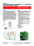
4 FUNCTIONAL BLOCK DIAGRAM Figure 1. AVDD1 AVSSGPIO0 GPIO1 XTAL1 CLKIO/XTAL2 DGNDREF REF+REFOUTAVDD2 REGCAPAAIN0 AIN1 AIN2 AIN3 AIN4 - CONTROLDIGITALFILTERAD7176-2 BUFFEREDPRECISIONREFERENCEXTAL AND INTERNALCLOCK OSCILLATORCIRCUITRYCSSCLKDINDOUT/RDYSYNC /ERROR11037-001 GPIO ANDMUXI/O CONTROLAD7176-2 Data Sheet Rev. D | Page 2 of 68 TABLE OF CONTENTS Features .. 1 Applications .. 1 General Description .. 1 Functional Block Diagram .. 1 Revision History .. 3 Specifications .. 4 Timing Characteristics .. 7 Timing Diagrams .. 7 Absolute Maximum Ratings .. 8 Thermal Resistance .. 8 ESD Caution .. 8 Pin Configuration and Function Descriptions .. 9 Typical Performance Characteristics .. 11 Noise Performance and Resolution .. 17 Getting Started .. 18 Power Supplies .. 19 Digital Communication .. 19 Configuration Overview .. 21 Circuit Description .. 26 analog Input.
5 26 Driver Amplifiers .. 26 AD7176-2 Reference .. 29 AD7176-2 Clock Source .. 30 Digital Filters .. 31 Sinc5 + Sinc1 31 Sinc3 Filter .. 32 Single Cycle settling .. 32 Enhanced 50 Hz and 60 Hz Rejection Filters .. 34 Operating Modes .. 37 Continuous Conversion Mode .. 37 Continuous Read Mode .. 38 Single Conversion Mode .. 39 Standby and Power-Down Modes .. 40 Calibration Modes .. 40 Digital Interface .. 41 Checksum 41 CRC Calculation .. 42 Integrated Functions .. 44 General-Purpose I/O .. 44 External Multiplexer Control .. 44 Delay .. 44 16-Bit/24-Bit 44 Serial Interface Reset (Dout_Reset) .. 44 Synchronization (SYNC/ERROR) .. 44 Error Flags .. 45 DATA _STAT .. 45 IOSTRENTGH .. 45 Grounding and Layout .. 46 Register Summary .. 47 Register Details .. 49 Communications Register .. 49 Status Register .. 50 ADC Mode Register .. 51 Interface Mode Register.
6 52 Register Check .. 53 Data Register .. 53 GPIO Configuration Register .. 54 ID 55 Channel Map Register 0 .. 56 Channel Map Register 1 .. 57 Channel Map Register 2 .. 58 Channel Map Register 3 .. 59 Setup Configuration Register 0 .. 60 Setup Configuration Register 1 .. 60 Setup Configuration Register 2 .. 61 Setup Configuration Register 3 .. 61 Filter Configuration Register 0 .. 62 Filter Configuration Register 1 .. 63 Filter Configuration Register 2 .. 64 Filter Configuration Register 3 .. 65 Offset Register 0 .. 66 Offset Register 1 .. 66 Offset Register 2 .. 66 Offset Register 3 .. 66 Gain Register 67 Gain Register 67 Gain Register 67 Gain Register 67 Outline Dimensions .. 68 Ordering Guide .. 68 Data Sheet AD7176-2 Rev. D | Page 3 of 68 REVISION HISTORY 3/16 Rev. C to Rev. D Changes to Power Supplies Section .. 19 Added AD7176-2 Reset Section.
7 20 6/15 Rev. B to Rev. C Changes to Figure 8 .. 11 10/14 R e v. A to R e v. B Changes to General Description .. 1 Changes to Figure 1 .. 1 Changes to Ta b l e 1 .. 4 Added ESD Rating (HBM) of kV; Table 3 and Changes t o Ta b l e 4 .. 8 Changes to Figure 5 to Figure 10 Captions .. 11 Changes to Figure 11 to Figure 16 Captions .. 12 Changes to Figure 17 to Figure 22 Captions .. 13 Changes to Figure 23 Caption; Added Figure 24 to Figure 28; Renumbered Sequentially .. 14 Added Figure 29 to Figure 34 .. 15 Added Figure 35 to Figure 36 .. 16 Changes to Noise Performance and Resolution Section .. 17 Changes to Getting Started Section and Figure 37 .. 18 Changes to Configuration Overview Section .. 21 Changes to Digital Filters Section and Table 19 .. 31 Changes to Sinc3 Filter Section .. 32 Changes to Table 20 .. 33 Reordered Figure 56 to Figure 63.
8 35 Changes to Figure 65 .. 38 Changes to Standby and Power-Down Modes Section .. 40 Changes to Digital Interface Section and Figure 68 .. 41 Changes to CRC Calculation Example .. 42 Added Integrated Function Section and Delay Section; Changes to General-Purpose I/O Section and Normal Synchronization Section .. 44 Changed Register 0x02 Bits[2:1] to HIDE_DELAY .. 47 Changes to Ta b l e 2 3 .. 49 Changes to Ta b l e 2 6 .. 52 Changes to Ta b l e 2 9 .. 54 Changes to Ta b l e 3 1 .. 56 Changes to Ta b l e 3 2 .. 57 Changes to Ta b l e 3 3 .. 58 Changes to Ta b l e 3 4 .. 59 Changes to Ta b l e 3 9 .. 62 Changes to Ta b l e 4 0 .. 63 Changes to Ta b l e 4 1 .. 64 Changes to Ta b l e 4 2 .. 65 4/13 to Rev. A Changes to Table 20 .. 31 11/12 Revision 0 Initial Version AD7176-2 Data Sheet Rev. D | Page 4 of 68 SPECIFICATIONS AVDD1 = V to V, AVDD2 = 2 V to V, IOVDD = 2 V to V, AVSS = DGND = 0 V, REF+ = V, REF = AVSS, internal master clock = 16 MHz, TA = TMIN to TMAX, unless otherwise noted.
9 Table 1. Parameter Test Conditions/Comments Min Typ Max Unit ADC SPEED AND PERFORMANCE Output Data Rate (ODR) 5 250,000 SPS No Missing Codes1 Excluding sinc3 filter 125 ksps 24 Bits Resolution See Table 6 Noise See Table 6 Noise Free Resolution Sinc5 + sinc1 filter (default) 250 ksps , REF+ = 5 V Bits ksps , REF+ = 5 V Bits 5 SPS, REF+ = 5 V Bits ACCURACY Integral Nonlinearity (INL) V reference 7 ppm of FSR 5 V reference 7 ppm of FSR Offset Error2 Internal short 40 V Offset Drift Internal short 110 nV/ C Offset Drift vs. Time3 450 nV/1000 hours Gain Error2 25 C 10 50 ppm/FSR Gain Drift vs. Temperature1 1 ppm/FSR/ C Gain Drift vs. Time3 3 ppm/FSR/ 1000 hours REJECTION Power Supply Rejection AVDD1, AVDD2 VIN = 1 V 90 dB Common-Mode Rejection VIN = V At DC 95 dB At 50 Hz and 60 Hz1 20 SPS ODR (post filter) (50 Hz 1 Hz and 60 Hz 1 Hz) 130 dB Normal Mode Rejection1 50 Hz 1 Hz and 60 Hz 1 Hz Internal clock, 20 SPS ODR (post filter) 71 90 dB External clock, 20 SPS ODR (post filter) 85 90 dB analog INPUTS Differential Input Voltage Range VREF V Absolute AIN Voltage Limits1 AVSS AVDD1 + V analog Input Current Input Current 48 A/V Input Current Drift External clock nA/V/ C Internal clock ( % clock)
10 4 nA/V/ C Crosstalk 1 kHz input 120 dB INTERNAL REFERENCE 100 nF external capacitor on REFOUT to AVSS Output Voltage REFOUT with respect to AVSS V Initial Accuracy1 TA = 25 C4 + V Temperature Coefficient 0 C to +105 C 2 5 ppm/ C 40 C to +105 C 3 10 ppm/ C Reference Load Current, ILOAD IL 10 +10 mA Power Supply Rejection (Line Regulation) AVDD1 and AVDD2 93 dB Load Regulation VOUT/ IL 32 ppm/mA Voltage Noise eN, Hz to 10 Hz V rms Voltage Noise Density eN, 1 kHz 215 nV/ Hz Turn-On settling Time 100 nF capacitor 60 s Data Sheet AD7176-2 Rev. D | Page 5 of 68 Parameter Test Conditions/Comments Min Typ Max Unit Long-Term Stability3 1000 hours 460 ppm Short Circuit ISC 25 mA EXTERNAL REFERENCE Reference Input Voltage Reference input = (REF+) (REF ) 1 AVDD1 V Absolute Reference Input Voltage Limits1 AVSS AVDD1 + V Average Reference Input Current 72 A/V Average Reference Input Current Drift External clock nA/V/ C Internal clock 6 nA/V/ C Normal Mode Rejection1 See the Rejection parameter section of this table Common-Mode Rejection 83 dB GENERAL-PURPOSE I/O (GPIO 0, GPIO 1)