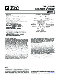
Transcription of 3-Axis, ±2 Data Sheet ADXL345 - Analog Devices
1 3-Axis, 2 g/ 4 g/ 8 g/ 16 g Digital Accelerometer data Sheet ADXL345 . FEATURES GENERAL DESCRIPTION. Ultralow power: as low as 23 A in measurement mode and The ADXL345 is a small, thin, ultralow power, 3-axis accelerometer A in standby mode at VS = V (typical) with high resolution (13-bit) measurement at up to 16 g. Digital Power consumption scales automatically with bandwidth output data is formatted as 16-bit twos complement and is acces- User-selectable resolution sible through either a SPI (3- or 4-wire) or I2C digital interface. Fixed 10-bit resolution The ADXL345 is well suited for mobile device applications. It Full resolution, where resolution increases with g range, measures the static acceleration of gravity in tilt-sensing appli- up to 13-bit resolution at 16 g (maintaining 4 mg/LSB. cations, as well as dynamic acceleration resulting from motion scale factor in all g ranges).
2 Or shock. Its high resolution ( mg/LSB) enables measurement Embedded memory management system with FIFO. of inclination changes less than . technology minimizes host processor load Single tap/double tap detection Several special sensing functions are provided. Activity and Activity/inactivity monitoring inactivity sensing detect the presence or lack of motion by Free-fall detection comparing the acceleration on any axis with user-set thresholds. Supply voltage range: V to V Tap sensing detects single and double taps in any direction. Free- I/O voltage range: V to VS fall sensing detects if the device is falling. These functions can SPI (3- and 4-wire) and I2C digital interfaces be mapped individually to either of two interrupt output pins. Flexible interrupt modes mappable to either interrupt pin An integrated memory management system with a 32-level first in, Measurement ranges selectable via serial command first out (FIFO) buffer can be used to store data to minimize host Bandwidth selectable via serial command processor activity and lower overall system power consumption.
3 Wide temperature range ( 40 C to +85 C) Low power modes enable intelligent motion-based power 10,000 g shock survival management with threshold sensing and active acceleration Pb free/RoHS compliant measurement at extremely low power dissipation. Small and thin: 3 mm 5 mm 1 mm LGA package The ADXL345 is supplied in a small, thin, 3 mm 5 mm 1 mm, APPLICATIONS 14-lead, plastic package. Handsets Medical instrumentation Gaming and pointing Devices Industrial instrumentation Personal navigation Devices Hard disk drive (HDD) protection FUNCTIONAL BLOCK DIAGRAM. VS VDD I/O. ADXL345 POWER. MANAGEMENT. CONTROL INT1. SENSE ADC AND. ELECTRONICS DIGITAL INTERRUPT. 3-AXIS FILTER LOGIC INT2. SENSOR. SDA/SDI/SDIO. 32 LEVEL. FIFO SERIAL I/O SDO/ALT. ADDRESS. SCL/SCLK. 07925-001. GND CS. Figure 1. Rev. E Document Feedback Information furnished by Analog Devices is believed to be accurate and reliable.
4 However, no responsibility is assumed by Analog Devices for its use, nor for any infringements of patents or other rights of third parties that may result from its use. Specifications subject to change without notice. No One Technology Way, Box 9106, Norwood, MA 02062-9106, license is granted by implication or otherwise under any patent or patent rights of Analog Devices . Tel: 2009 2015 Analog Devices , Inc. All rights reserved. Trademarks and registered trademarks are the property of their respective owners. Technical Support ADXL345 data Sheet TABLE OF CONTENTS. Features .. 1 Self-Test .. 22. Applications .. 1 Register Map .. 23. General Description .. 1 Register Definitions .. 24. Functional Block Diagram .. 1 Applications Information .. 28. Revision History .. 3 Power Supply Decoupling .. 28. 4 Mechanical Considerations for Mounting.
5 28. Absolute Maximum 6 Tap Detection .. 28. Thermal Resistance .. 6 Threshold .. 29. Package Information .. 6 Link Mode .. 29. ESD Caution .. 6 Sleep Mode vs. Low Power 30. Pin Configuration and Function Descriptions .. 7 Offset Calibration .. 30. Typical Performance Characteristics .. 8 Using Self-Test .. 31. Theory of Operation .. 13 data Formatting of Upper data Rates .. 32. Power Sequencing .. 13 Noise Performance .. 33. Power Savings .. 14 Operation at Voltages Other Than V .. 33. Serial Communications .. 15 Offset Performance at Lowest data Rates .. 34. SPI .. 15 Axes of Acceleration Sensitivity .. 35. I2C .. 18 Layout and Design Recommendations .. 36. Interrupts .. 20 Outline Dimensions .. 37. FIFO .. 21 Ordering Guide .. 37. Rev. E | Page 2 of 40. data Sheet ADXL345 . REVISION HISTORY. 6/15 Rev. D to Rev. E Changes to Figure 36 to Figure 38.
6 15. Changes to Features Section and General Changes to Table 9 and Table 10 .. 16. Description Section .. 1 Changes to I2C Section and Table 11 .. 17. Change to Figure 36 ..15 Changes to Table 12 .. 18. Change to FIFO Section ..21 Changes to Interrupts Section, Activity Section, Inactivity Section, and FREE_FALL 19. 2/13 Rev. C to Rev. D Added Table 13 .. 19. Changes to Figure 13, Figure 14, and Figure 15 .. 9 Changes to FIFO Section .. 20. Change to Table 15 ..22 Changes to Self-Test Section and Table 15 to Table 18 .. 21. Added Figures 42 and Table 14 .. 21. 5/11 Rev. B to Rev. C Changes to Table 19 .. 22. Added Preventing Bus Traffic Errors Section ..15 Changes to Register 0x1D THRESH_TAP (Read/Write). Changes to Figure 37, Figure 38, Figure 39 ..16 Section, Register 0x1E, Register 0x1F, Register 0x20 OFSX, Changes to Table 12.
7 19 OFSY, OSXZ (Read/Write) Section, Register 0x21 DUR. Changes to Using Self-Test (Read/Write) Section, Register 0x22 Latent (Read/Write). Changes to Axes of Acceleration Sensitivity Section, and Register 0x23 Window (Read/Write) Section .. 23. Changes to ACT_X Enable Bits and INACT_X Enable Bit 11/10 Rev. A to Rev. B Section, Register 0x28 THRESH_FF (Read/Write) Section, Change to 0 g Offset vs. Temperature for Z-Axis Parameter, Register 0x29 TIME_FF (Read/Write) Section, Asleep Bit Table 1 .. 4 Section, and AUTO_SLEEP Bit 24. Changes to Figure 10 to Figure 15 .. 9 Changes to Sleep Bit Section .. 25. Changes to Ordering Guide ..37 Changes to Power Supply Decoupling Section, Mechanical Considerations for Mounting Section, and Tap Detection 4/10 Rev. 0 to Rev. A Section .. 27. Changes to Features Section and General Changes to Threshold 28.
8 Description Section .. 1 Changes to Sleep Mode vs. Low Power Mode Section .. 29. Changes to Specifications 3 Added Offset Calibration Section .. 29. Changes to Table 2 and Table 3 .. 5 Changes to Using Self-Test Section .. 30. Added Package Information Section, Figure 2, and Table 4; Added data Formatting of Upper data Rates Section, Figure 48, Renumbered Sequentially .. 5 and Figure 49 .. 31. Changes to Pin 12 Description, Table 5 .. 6 Added Noise Performance Section, Figure 50 to Figure 52, and Added Typical Performance Characteristics Section .. 7 Operation at Voltages Other Than V Section .. 32. Changes to Theory of Operation Section and Power Sequencing Added Offset Performance at Lowest data Rates Section and Section ..12 Figure 53 to Figure 55 .. 33. Changes to Powers Savings Section, Table 7, Table 8, Auto Sleep Mode Section, and Standby Mode Section.
9 13 6/09 Revision 0: Initial Version Changes to SPI Section ..14. Rev. E | Page 3 of 40. ADXL345 data Sheet SPECIFICATIONS. TA = 25 C, VS = V, VDD I/O = V, acceleration = 0 g, CS = 10 F tantalum, CI/O = F, output data rate (ODR) = 800 Hz, unless otherwise noted. All minimum and maximum specifications are guaranteed. Typical specifications are not guaranteed. Table 1. Parameter Test Conditions Min Typ1 Max Unit SENSOR INPUT Each axis Measurement Range User selectable 2, 4, 8, 16 g Nonlinearity Percentage of full scale %. Inter-Axis Alignment Error Degrees Cross-Axis Sensitivity2 1 %. OUTPUT RESOLUTION Each axis All g Ranges 10-bit resolution 10 Bits 2 g Range Full resolution 10 Bits 4 g Range Full resolution 11 Bits 8 g Range Full resolution 12 Bits 16 g Range Full resolution 13 Bits SENSITIVITY Each axis Sensitivity at XOUT, YOUT, ZOUT All g-ranges, full resolution 230 256 282 LSB/g 2 g, 10-bit resolution 230 256 282 LSB/g 4 g, 10-bit resolution 115 128 141 LSB/g 8 g, 10-bit resolution 57 64 71 LSB/g 16 g, 10-bit resolution 29 32 35 LSB/g Sensitivity Deviation from Ideal All g-ranges %.
10 Scale Factor at XOUT, YOUT, ZOUT All g-ranges, full resolution mg/LSB. 2 g, 10-bit resolution mg/LSB. 4 g, 10-bit resolution mg/LSB. 8 g, 10-bit resolution mg/LSB. 16 g, 10-bit resolution mg/LSB. Sensitivity Change Due to Temperature %/ C. 0 g OFFSET Each axis 0 g Output for XOUT, YOUT 150 0 +150 mg 0 g Output for ZOUT 250 0 +250 mg 0 g Output Deviation from Ideal, XOUT, YOUT 35 mg 0 g Output Deviation from Ideal, ZOUT 40 mg 0 g Offset vs. Temperature for X-, Y-Axes mg/ C. 0 g Offset vs. Temperature for Z-Axis mg/ C. NOISE. X-, Y-Axes ODR = 100 Hz for 2 g, 10-bit resolution or LSB rms all g-ranges, full resolution Z-Axis ODR = 100 Hz for 2 g, 10-bit resolution or LSB rms all g-ranges, full resolution OUTPUT data RATE AND BANDWIDTH User selectable Output data Rate (ODR)3, 4, 5 3200 Hz SELF-TEST6. Output Change in X-Axis g Output Change in Y-Axis g Output Change in Z-Axis g POWER SUPPLY.
